How to Design 5G PCB and Material Selection
The world is speeding up the adoption of 5G networks, which promise faster internet, quicker connections and the ability to link up tons of devices. Making these networks work are special circuit boards called 5G PCBs. They help send out 5G signals and handle the high frequencies needed for 5G.
But designing these circuit boards isn’t easy. They have to deal with higher frequencies than before. To make them work, engineers need to pick the right materials and carefully plan how everything fits together to avoid problems like losing signals or overheating.
This guide is like a roadmap for engineers. It covers things like:
- Understanding what frequencies 5G uses and how fast it needs to go
- Choosing the best materials for the circuit board
- Figuring out the best way to lay everything out for a strong connection
- Making sure things don’t get too hot
- Keeping interference and signal loss to a minimum
- Testing everything to make sure it works right
By the end of the guide, engineers will know how to design and improve 5G circuit boards to make the most of what 5G can do.
5G Frequency Data Rates and Band Rates
5G networks use different frequencies compared to older wireless tech. They use high-frequency bands called millimeter waves (mmWave) between 24 GHz to 52 GHz, and also some lower sub-6 GHz frequencies.
MmWave frequencies have lots of available spectrum, allowing for super-fast data rates. Some mmWave bands used for 5G include:
- n257 (28 GHz)
- n258 (26 GHz)
- n261 (27.5 GHz – 28.35 GHz)
Here are some key 5G frequency bands and their speeds:
| Frequency Band | Data Rate |
|---|---|
| 600 MHZ | 1000 Mbps |
| 2.5 GHz | 1 Gbps |
| 4.7 GHz | 1.3 Gbps |
| 24 GHz | 3 Gbps |
| 28 GHz | 5 Gbps |
| 39 GHz | 7 Gbps |
But, the higher frequency mmWave signals have shorter wavelengths and don’t go through obstacles easily. This means they lose signal strength more quickly, which needs advanced antenna tech like massive MIMO and beamforming.
When making a 5G PCB, it’s crucial to think about the frequency bands and speed needs. The board has to handle high-frequency signals well, with good gain and minimal signal loss.
PCB Substrate Materials
Let’s explore the key properties of PCB substrate materials for 5G, including dielectric constant, loss tangent, thermal conductivity, coefficient of thermal expansion (CTE), moisture absorption and thickness.
Dielectric Constant
The dielectric constant, also known as the relative permittivity, is a measure of a material’s ability to store electrical energy in an electric field. In PCBs, the dielectric constant determines the speed at which electrical signals can propagate through the substrate material. For 5G applications, it is important to choose a substrate material with a low dielectric constant to minimize signal loss and ensure high-speed data transmission.
Substrate materials such as polytetrafluoroethylene (PTFE), commonly known as Teflon, have a low dielectric constant, making them suitable for high-frequency applications like 5G. Other materials like FR-4, a widely used epoxy-based substrate material, have a higher dielectric constant, which may limit their use in certain 5G applications.
Loss Tangent
The loss tangent, also known as the dissipation factor, is a measure of the energy lost as heat when an electrical signal passes through a material. It is an important parameter for high-frequency applications like 5G, as it directly affects the signal integrity and power efficiency of the PCB.
Low-loss substrate materials with a low loss tangent are preferred for 5G applications to minimize signal attenuation and ensure reliable data transmission. Materials like PTFE and liquid crystal polymer (LCP) offer low-loss characteristics, making them suitable for high-frequency PCB designs.
Thermal Conductivity
Thermal management is crucial in electronic devices, especially in high-power applications like 5G. The thermal conductivity of a substrate material determines its ability to dissipate heat generated by the components on the PCB. A substrate material with high thermal conductivity helps in efficient heat dissipation, preventing overheating and ensuring the reliability of the PCB.
Copper-based substrate materials, such as metal-core printed circuit boards (MCPCBs), offer excellent thermal conductivity and are commonly used in high-power applications. However, for 5G applications where size and weight are critical, alternative materials like ceramic-filled PTFE can provide a balance between thermal performance and weight reduction.
Coefficient of Thermal Expansion (CTE)
The coefficient of thermal expansion (CTE) is a measure of how much a material expands or contracts with changes in temperature. In PCBs, CTE mismatch between the substrate material and the components can lead to stress, delamination, and reliability issues.
For 5G applications, it is important to choose a substrate material with a CTE that closely matches that of the components to minimize the risk of thermal stress-induced failures. Materials like FR-4 have a CTE that is well-matched with common electronic components, making them a popular choice for 5G PCBs.
Moisture Absorption
Moisture absorption is an important consideration for PCBs, as excessive moisture can lead to electrical failures and reliability issues. Moisture can penetrate the substrate material through microcracks, voids, or exposed edges, causing degradation of the electrical properties and potential short circuits.
For 5G applications, it is crucial to choose a substrate material with low moisture absorption to ensure the long-term reliability of the PCB. Materials like PTFE and LCP have low moisture absorption properties, making them suitable for 5G applications where reliability is paramount.
Thickness
Thinner dielectrics play a imp role in minimizing signal loss at mmWave frequencies. The thickness of these dielectrics varies based on the number of layers, but for 5G, substrates typically range between 0.1mm to 0.3mm in thickness.
Here’s a comparison of various popular 5G PCB substrate materials and their characteristics:
| Material | DK | Loss Tangent | Thermal Conductivity | CTE | Moisture Absorption |
|---|---|---|---|---|---|
| Rogers R03003 | 3.0 | 0.0013 | 0.31 W/mk | 17 ppm/°c | 0.06% |
| Rogers R04835 | 3.33 | 0.0031 | 0.74 W/mk | 11 ppm/°c | 0.04% |
| Taconic RF-35A2 | 3.5 | 0.0018 | 0.69 W/mk | 7 ppm/°c | 0.02% |
| Polyimide | 3.4-3.6 | 0.002-0.004 | 0.12 W/mk | 20-70 ppm/°c | 1-4% |
| PTFE | 2.1 | 0.0002 | 0.25 W/mk | 17 ppm/°c | 0% |
| LCP | 2.9 | 0.0025 | 0.67 W/mk | 17 ppm/°c | 0.04% |
| Aluminum Nitride | 8.9 | 0.0001 | 170 W/mk | 4.3 ppm/°c | 0% |
Layer Stackup Design
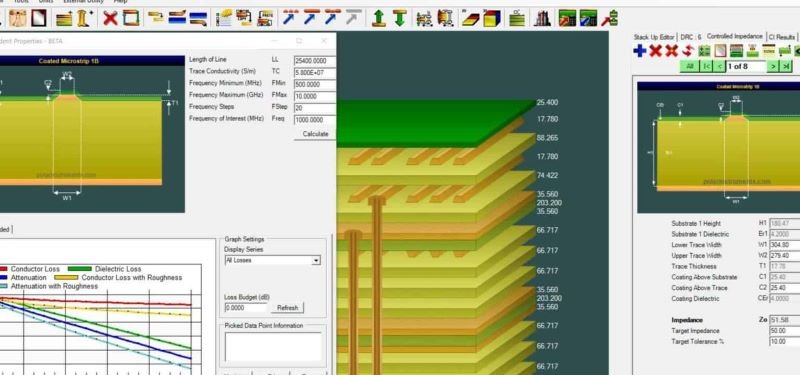
The layer stackup determines how many copper and dielectric layers are in a PCB. Getting the stackup right is crucial for controlling impedance, reducing loss, and maintaining signal quality at 5G frequencies. Here are some important tips for designing 5G PCB stackups:
- Use thicker copper layers (2oz/ft2 or more) to cut down on conductive losses.
- Try to minimize the number of lamination cycles to keep signal loss to a minimum.
- Place ground planes close to signal layers to control impedance.
- Keep the layer count low, usually between 4-8 layers, for the best 5G performance.
- Use symmetric stripline setups for differential pairs.
- Pay attention to layer transitions using tapers/chamfers.
- Consider a split power plane setup to separate noise-sensitive power supplies.
- Make sure there are thermal vias under hot components to dissipate heat effectively.
An example of an 8-layer stackup for a high-frequency 5G board could be:
| Layer | Function | Thickness |
|---|---|---|
| 1 | Signal | 2 oz Cu |
| 2 | Ground | 1 oz Cu |
| 3 | Power | 2 oz Cu |
| 4 | Signal | 2 oz Cu |
| 5 | Ground | 1 oz Cu |
| 6 | Power | 2 oz Cu |
| 7 | Ground | 1 oz Cu |
| 8 | Signal | 2 oz Cu |
Having ground planes close together helps manage impedance, lower EMI (Electromagnetic Interference), and reduce crosstalk. Splitting power planes isolates digital and analog power sources. Thicker copper layers (2oz or more) cut down on conduction losses.
5G PCB Layout Guidelines
Designing a PCB layout for 5G applications requires careful consideration of several factors, including controlled impedance, isolation between RF and digital components, minimizing trace lengths, EMI shielding, power delivery network, thermal management, antenna integration, and test points. In this article, we will explore each of these guidelines to help you create a high-performance PCB layout for your 5G project.
Controlled Impedance
Controlled impedance is crucial for ensuring signal integrity in high-speed digital and RF circuits. In 5G applications, where data rates are significantly higher, maintaining controlled impedance becomes even more critical. To achieve controlled impedance, you need to carefully select the PCB stack-up, trace width, and dielectric material. Consult the datasheets of your components and use a reliable impedance calculator to determine the appropriate trace width and spacing.
Isolation Between RF and Digital
In 5G PCB designs, it is essential to maintain proper isolation between RF and digital components to prevent interference and crosstalk. Place RF and digital components on separate PCB layers and use ground planes and shielding techniques to minimize coupling. Additionally, keep the RF traces as short as possible and use guard traces or guard rings to further isolate sensitive RF signals.
Minimize Trace Lengths
Reducing trace lengths is crucial for minimizing signal degradation and improving signal integrity. In 5G PCB layouts, where high-frequency signals are prevalent, it is even more important to keep trace lengths as short as possible. Use a compact layout and place components strategically to minimize the length of critical signal traces. Consider using differential signaling for high-speed data lines to further improve signal integrity.
EMI Shielding
Electromagnetic interference (EMI) can significantly impact the performance of 5G systems. To minimize EMI, you need to incorporate effective shielding techniques in your PCB layout. Use grounded planes and partitions to isolate sensitive components and signals. Place EMI filters strategically to suppress high-frequency noise. Additionally, ensure proper grounding and use shielding cans or conductive enclosures wherever necessary.
Power Delivery Network
A robust power delivery network is essential for reliable operation of 5G systems. Ensure sufficient power and ground planes to minimize voltage drops and noise. Use decoupling capacitors near power pins of ICs to provide local charge storage and reduce power supply noise. Consider using power integrity analysis tools to optimize the power distribution network and minimize power-related issues.
Thermal Management
5G applications generate a significant amount of heat due to high data rates and processing power. Proper thermal management is crucial to prevent overheating and ensure reliable operation. Place thermal vias near heat-generating components to dissipate heat efficiently. Use thermal pads or heat sinks to enhance heat dissipation. Ensure proper airflow and consider using fans or heat pipes for active cooling if necessary.
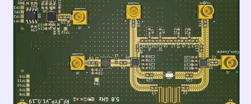
Antenna Integration
Integrating antennas into the PCB layout is a critical aspect of 5G designs. Carefully select the antenna type and position it optimally for maximum signal strength and coverage. Ensure proper impedance matching between the antenna and the transmission line to minimize signal loss. Consider using RF connectors or antenna feed lines with controlled impedance for better performance.
Test Points
Test points are essential for debugging, testing, and troubleshooting PCB designs. Incorporate sufficient test points in your 5G PCB layout to facilitate easy access to critical signals and test points. These test points can be used for measuring signal quality, debugging firmware, or performing functional tests. Place test points strategically to ensure easy access without interfering with the overall layout.
Mitigating Loss and Signal Integrity
Reducing loss and ensuring signal integrity is crucial for 5G PCBs, especially with the higher frequencies involved compared to 4G or Wi-Fi. Here are some methods to help address loss and enhance signal performance:
- Extensive Ground Stitches: Connecting all ground areas with many via and microvia stitches decreases ground inductance.
Backdrilling (Via Stub Removal): Removing unused parts of plated through holes enhances impedance matching and decreases reflections. - Buried/Blind Vias: Using vias spanning only 2-3 layers controls coupling compared to full-depth drilled vias.
- Smooth Layer Transitions: Tapered chamfers/rounded corner pads on layer transitions prevent sudden impedance changes.
- Spacing from Ground: Keeping sufficient clearance from ground layers prevents energy loss through substrate radiation.
- Matched Length Routing: Adjusting trace lengths to match electrical lengths improves insertion loss in differential pairs.
- Periodic Voiding: Introducing voids along a reference plane reduces eddy current losses at high frequencies.
- Dielectric Coatings: Applying low-loss tangent coatings like paralene or PTFE on traces minimizes surface wave propagation loss.
By carefully modeling and simulating these techniques, engineers can fine-tune 5G board performance.
Thermal Management Approaches
Effective heat dissipation is crucial for 5G PCBs, especially with increased power densities at mmWave frequencies. Here are some methods to manage heat effectively:
- Metal Core Substrates: These substrates have aluminum or copper bases to spread heat.
- Thermal Vias: Drilled holes filled with metallization conduct heat to inner layers.
- Heatsinks/Heat-Spreaders: Machined aluminum heatsinks with thermal interface material help dissipate heat.
- Fans/Air Flow: Incorporating small fans or ventilation channels into the enclosure aids in cooling.
- Phase Change Materials: Substrates with materials that change phase to absorb heat.
- Vapor Chambers: Hollow chambers with working fluid that evaporates and condenses, transferring heat.
Ideally, these thermal management techniques should be modeled during the design phase to predict temperature changes and optimize heat flow.
EMI Control Methods
Controlling electromagnetic interference (EMI) is vital in 5G designs to avoid disrupting other devices and to meet EMI/EMC standards. Here are some methods to control EMI:
- Metal Shielding Cans: Placing metal shields over sensitive ICs helps contain electromagnetic emissions.
- Waveguide Vents: Using small aperture waveguide vents on enclosures allows controlled release of electromagnetic energy.
- Ground Plane Stitching: Strategic placement of ground vias across multiple layers forms “walls” to contain electromagnetic interference.
- Filtering Components: Adding components like ferrite beads on I/O helps filter out unwanted electromagnetic noise.
- Shielding Gaskets: Applying additional shielding gaskets on enclosure seams enhances containment of electromagnetic radiation.
- Internal Metal Compartmentalization: Partitioning the internal space with metal helps prevent the formation of slot antennas.
- Careful Component Placement: Thoughtful placement of components helps keep noise sources contained.
- Sparse Power Plane Fills: Leaving islands disconnected at DC on power planes reduces the spread of electromagnetic interference.
Prototyping and testing are crucial to validate EMI performance. It often involves an iterative process of identifying issues and implementing fixes. Shielding, filtering, and isolation are fundamental principles for effective EMI and EMC management.
Testing and Validation
Testing and validation are crucial steps in the PCB development process to ensure optimal performance. Here are some methods used for testing and validation:
- Simulation and Modeling: Use 3D EM simulations to analyze traces, stackup, power distribution network (PDN), and thermal performance. Identify potential issues through modeling.
- Frequency Sweeps: Utilize a network analyzer to measure insertion loss, return loss, and impedance across different frequencies. Verify signal magnitude and phase consistency.
- VSWR and Losses: Evaluate voltage standing wave ratio (VSWR), gain, and losses to detect impedance mismatches and unexpected resonances.
- Eye Diagrams: Analyze eye diagrams to assess signal integrity and jitter. A clear, open eye indicates clean signaling.
- Time Domain Reflectometry (TDR): Use TDR plots to identify impedance mismatches and discontinuities along traces caused by reflections. Useful for controlled impedance validation.
- Vibration/Shock Testing: Assess mechanical robustness under vibration and shock conditions to check for solder joint cracks or trace/via fractures.
- Thermal Imaging: Employ an infrared (IR) thermal imaging camera to map hot spots and temperature gradients on the board. Identify areas with cooling deficiencies.
- EMI Diagnostics: Test for radiated and conducted EMI compliance to identify specific noise sources.
Conclusion
In simpler terms, designing circuit boards for 5G is tricky because of the new high-frequency technology. But with careful planning and using the right materials and layout, we can make boards that work really well. By following the advice in this article, designers can help make 5G networks faster and more reliable. It’s all about making sure the signals stay strong, managing heat, and avoiding interference.