How to Read a PCB Schematic?
Reading a PCB (Printed Circuit Board) schematic is an essential skill for anyone involved in electronics or circuit design. A PCB schematic is a graphical representation of an electronic circuit, showing the connections between various components and their functions. It serves as a blueprint for the physical layout of the circuit on the PCB.
How to read a PCB schematic?
Understanding a PCB schematic involves grasping the interconnection of components depicted on it. It encompasses details about different components and the circuit’s operational parameters. The schematic furnishes the following insights:
- Identification of components utilized.
- Depiction of electrical interconnections among component pins.
- Specification of operational conditions like voltage, current, and tolerances.
- Inclusion of special directives such as single-ended impedance traces, differential pairs, and component placement particulars like the positioning of decoupling capacitors, crystals, etc.
- Illustration of a block diagram outlining the system’s architecture.
- Documentation of revision history, if applicable.
Understanding Schematic Nets, Junctions, and Net Naming
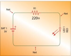
In a PCB schematic, nets represent the electrical connections between components. They are usually denoted by lines or wires connecting the various symbols representing the components. Each net has a unique name or label, which helps identify and trace its path throughout the circuit.
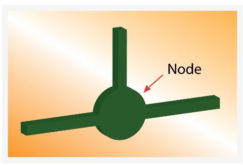
Junctions, on the other hand, are points where multiple nets intersect or connect. They are usually represented by dots or small circles. Junctions ensure that the electrical connections are properly made and that signals can flow between different parts of the circuit.
Net naming is an important aspect of PCB schematics. Each net should have a clear and descriptive name that reflects its purpose or function in the circuit. This makes it easier to understand and troubleshoot the circuit during the design and manufacturing process.
The Difference Between Schematic Diagram and Layout
While a PCB schematic represents the logical and functional aspects of a circuit, the layout refers to the physical arrangement of components and their connections on the actual PCB. The layout is a detailed representation of how the components are placed and interconnected on the board.
A schematic diagram focuses on the circuit’s functionality, showing the relationships between components and their electrical connections. It helps in understanding the overall circuit design and how different components interact with each other.
On the other hand, the PCB layout is concerned with the physical implementation of the circuit. It takes into account factors such as component footprints, trace routing, power and ground planes, and signal integrity. The layout ensures that the circuit functions as intended and meets the required electrical and mechanical specifications.
While the schematic diagram provides a high-level view of the circuit, the layout is a more detailed representation that takes into consideration the physical constraints and manufacturing requirements of the PCB.
Tips for Reading a PCB Schematic
Here are some tips to help you read and understand a PCB schematic:
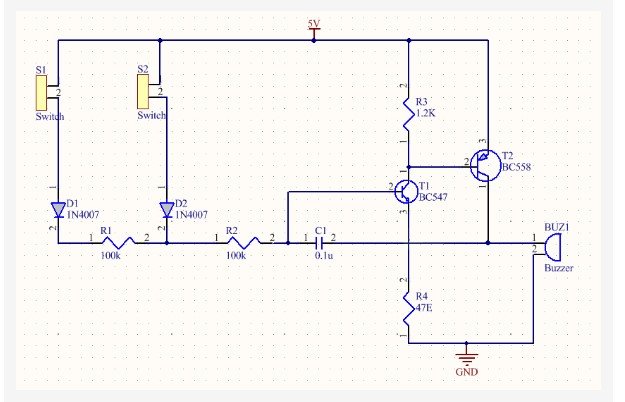
- Start by identifying the key components in the circuit and their symbols. This includes resistors, capacitors, transistors, integrated circuits, and any other active or passive components.
- Pay attention to the net names and labels. They provide valuable information about the purpose and function of each connection in the circuit.
- Follow the flow of signals through the circuit. Trace the paths of the nets to understand how the different components are interconnected.
- Refer to the component datasheets for a better understanding of their pin configurations and functionalities.
- Look for reference designators, which are unique identifiers assigned to each component in the schematic. These help in locating the corresponding components on the PCB layout.
- Understand the different symbols and notations used in the schematic. This includes power supply symbols, ground symbols, test points, and any special symbols specific to the circuit.
- Use the schematic as a guide when troubleshooting or debugging the circuit. It can help you identify potential issues or faulty connections.
Rules for Drawing a Schematic Diagram
1. Use Standard Symbols: It’s crucial to use standard symbols for components such as resistors, capacitors, diodes, transistors, and integrated circuits. These symbols are universally recognized and ensure clarity in communication.
2. Follow a Logical Flow: Arrange the components in a logical flow from left to right or top to bottom, following the direction of the current flow. This makes it easier to comprehend the circuit’s operation.
3. Label Components Clearly: Ensure that each component is labeled clearly with its respective designator (e.g., R1 for resistor 1, C1 for capacitor 1) and value. This aids in easy identification and troubleshooting.
4. Use Consistent Spacing: Maintain consistent spacing between components and connections to enhance the diagram’s readability. Neat and organized layouts make it easier to understand complex circuits.
5. Draw Straight Lines: Use straight lines to connect components, and avoid overlapping lines to prevent confusion. Crossing lines should be minimized, and when necessary, use a dot or bridge to indicate a connection.
Creating a Schematic Diagram
Now, let’s delve into the process of creating a schematic diagram:
1. Identify Components: Begin by identifying all the components that will be part of the circuit. This includes active components like transistors and integrated circuits, as well as passive components such as resistors, capacitors, and inductors.
2. Understand the Circuit Operation: Gain a clear understanding of how the circuit is intended to function. This comprehension will guide the placement and interconnection of components in the schematic diagram.
3. Choose the Right Tool: Select a suitable software or tool for creating the schematic diagram. There are various options available, ranging from specialized electronic design automation (EDA) tools to simple schematic capture software.
4. Place Components: Begin placing the components on the workspace provided by the software. As per the logical flow, arrange the components in a manner that reflects their actual physical or functional placement in the circuit.
5. Connect the Components: Use the appropriate tool within the software to connect the components with lines representing conductive paths. Ensure that the connections accurately reflect the intended electrical connections in the circuit.
6. Label and Annotate: Label each component with its designator and value. Additionally, annotate the components to assign unique reference designators automatically, ensuring there are no conflicts.
7. Review and Edit: Thoroughly review the schematic diagram for accuracy, completeness, and clarity. Make any necessary edits to improve the overall readability and understanding of the circuit.
By following these rules and steps, you can create a clear and comprehensive schematic diagram that effectively communicates the structure and operation of the circuit.