CD4049: The Features, Applications and Circuit Diagram
Introduction to the CD4049 Hex Inverting Buffer IC
The CD4049, also called HEF4049B or MC14049B, is a fast electronic chip that can change signals in a circuit. It’s like a versatile tool that’s commonly used in many electronic devices because it can do things like flipping signals and helping to control large loads. In this article, we’ll take a closer look at what the CD4049 chip can do, where it’s used, and how it’s connected in a circuit.
Features of the CD4049
The CD4049 is a hex inverter/buffer IC that consists of six independent inverters. Here are some of its notable features:
- CMOS Technology: The CD4049 is made using Complementary Metal-Oxide-Semiconductor (CMOS) technology, which is great because it uses very little power and can handle noise well.
- Six Independent Inverters: Inside the chip, there are six separate parts called inverters. Each one can do its own job, like flipping signals, and they’re all packed into one tiny package.
- Fast Operation: This chip works really quickly, with a typical delay of just 60 nanoseconds. That means it’s perfect for speedy digital circuits.
- Wide Voltage Range: It’s flexible with power – you can use it with anything from 3 volts to 15 volts, which means it fits well with different power setups.
- Strong Output: Each inverter is tough – it can handle driving up to 10 other loads or 50 picofarads of capacitance, which means it can send signals reliably.
- High Input Sensitivity: The CD4049 is good at listening – it has a high input sensitivity, so it won’t disrupt the signals it’s receiving.
- Schmitt-Trigger Action: These inverters are smart – they have something called Schmitt-trigger action, which helps them handle noise better and keep signals clear.
Applications of the CD4049
The CD4049 finds applications in various electronic circuits and systems. Here are some of its common uses:
- Signal Conditioning: The CD4049 can be used for signal conditioning, such as amplification, level shifting, and waveform shaping. Its inverters can be configured to modify input signals according to the desired output requirements.
- Logic Level Shifting: In mixed-voltage systems, the CD4049 can be used for logic level shifting, allowing communication between devices operating at different voltage levels.
- Oscillators: By connecting the inverters in a feedback configuration, the CD4049 can be used to build oscillators for generating clock signals or square wave signals.
- Waveform Generation: The CD4049 can generate various waveforms, including square waves, triangular waves, and pulse waves, by utilizing its inverters in different configurations.
- Buffering: The CD4049 can be used as a buffer to isolate and amplify signals, ensuring proper signal transmission between different sections of a circuit.
- Motor Control: The CD4049 can be employed in motor control circuits to drive and control the speed of motors, making it useful in robotics and automation applications.
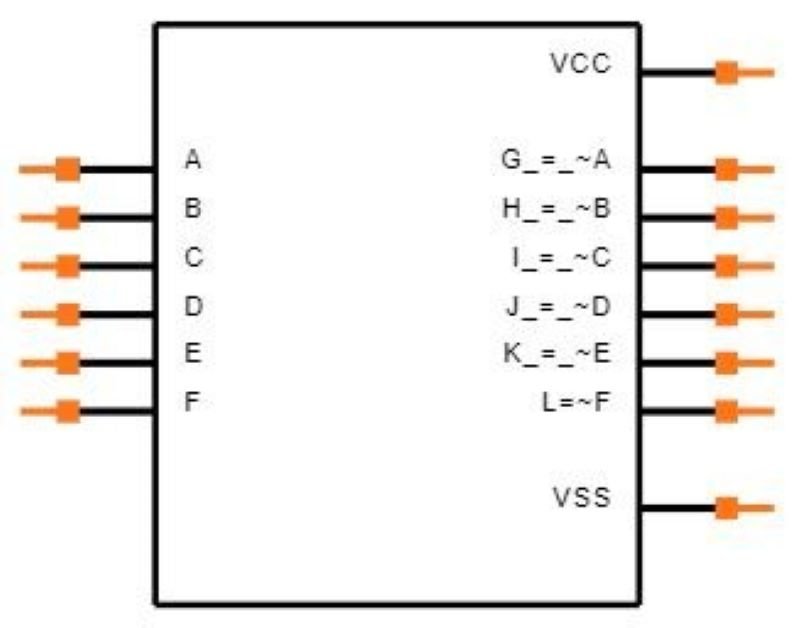
Pin Configuration and Function Table
The CD4049 IC is packaged in a 16-pin Dual In-Line Package (DIP). Here’s how the pins are arranged and what they do:
| Pin Number | Pin Name | Function |
|---|---|---|
| 1 | 1A | Input of Inverter 1 |
| 2 | 1Y | Output of Inverter 1 |
| 3 | 2A | Input of Inverter 2 |
| 4 | 2Y | Output of Inverter 2 |
| 5 | 3A | Input of Inverter 3 |
| 6 | 3Y | Output of Inverter 3 |
| 7 | VSS | Ground (negative supply) |
| 8 | 4Y | Output of inverter 4 |
| 9 | 4A | Input of inverter 4 |
| 10 | 5Y | Output of inverter 5 |
| 11 | 5A | Input of inverter 5 |
| 12 | 6Y | Output of Inverter 6 |
| 13 | 6A | Input of inverter 6 |
| 14 | VDD | Positive Supply Voltage |
| 15 | NC | No connection |
| 16 | NC | No connection |
Logic Diagram and Truth Table
The logic diagram of the CD4049 shows six separate inverters inside the chip. Each inverter has two connections: one for input (labeled as A) and one for output (labeled as Y). Here’s what happens inside each inverter, as shown in the truth table:
| Input (A) | Output (Y) |
|---|---|
| 0 | 1 |
| 1 | 0 |
Circuit Diagram and Example Applications
Inverting Buffer Circuit
A basic application of the CD4049 involves using it as an inverting buffer. Here’s a simple circuit diagram illustrating how a single inverter can be used as an inverting buffer:
         VDD
          |
          |
     +----+----+
     |    1    |
     |    |    |
Input|----+----|Input  Output|----+-----Output
     |         |             |    |
     |         |             |    |
     +---------+             +----+
          |
          |
         GND
In this setup, the input signal undergoes inversion and buffering through the inverter, resulting in a tidy and inverted output signal.
Conclusion
In conclusion, The CD4049 is a versatile IC with a wide range of applications in the field of electronics. Its features, such as a wide operating voltage range, low power consumption, and high noise immunity, make it suitable for diverse projects and systems. By utilizing its inverters, the CD4049 can be employed for signal conditioning, logic level shifting, waveform generation, buffering, and motor control, among other applications. The circuit diagram provided offers a basic understanding of how the CD4049 can be used as an inverter, but it can be configured in various other ways to suit different requirements.