
What is Multilayer PCB? Definition, Manufacturing Process and Uses
Single-layer and double-layer PCBs are commonly used, there are also multilayer PCBs that offer enhanced functionality and versatility. A multilayer PCB, also known as a multilayer printed circuit board, is a type of circuit board that consists of multiple layers of conductive material separated by insulating layers. These boards are used in a wide range of electronic devices and are known for their compactness and high functionality. In this article, we will explore what multilayer PCBs are and why they are important in modern electronics.
What is Multilayer PCB?
A multilayer PCB, as the name suggests, is a circuit board that consists of multiple layers of conductive traces and insulating material. Unlike single-layer or double-layer PCBs, which have only one or two layers respectively, multilayer PCBs can have three or more layers. These layers are stacked on top of each other and interconnected through vias, which are small holes filled with conductive material.
Each layer of a multilayer PCB is typically made of a thin copper foil, which acts as a conductor. The layers are separated by a layer of insulating material, such as epoxy resin or fiberglass, which prevents electrical interference between the different layers. The number of layers in a multilayer PCB can vary depending on the complexity of the circuit and the specific requirements of the electronic device.
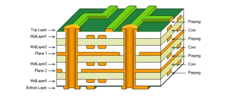
The Structure of Multilayer PCB Boards
1. Core Layers:
The core layers are the innermost layers of the multilayer PCB. They are made up of a thin layer of copper foil laminated onto an insulating substrate. The core layers provide the foundation for the circuitry and serve as the base for the other layers to be built upon.
2. Prepreg Layers:
Prepreg layers are layers of fiberglass or epoxy resin that are impregnated with a resin adhesive. These layers are placed on top of the core layers and act as insulation between the copper layers. The prepreg layers also help to strengthen the overall structure of the PCB.
3. Copper Layers:
The copper layers in a multilayer PCB are the conductive layers that carry the electrical signals. These layers consist of thin sheets of copper foil that are laminated onto the prepreg layers. The copper layers are etched to create the desired circuit pattern, and the excess copper is removed, leaving only the traces and pads needed for the circuit.
4. Soldermask Layers:
The soldermask layers are applied on top of the copper layers to protect the circuitry from environmental factors such as moisture, dust, and corrosion. The soldermask is typically a green color, but it can also be other colors such as red, blue, or black. It also helps to prevent solder bridges between adjacent copper traces during the soldering process.
5. Silkscreen Layers:
The silkscreen layers are used to add labels, symbols, and component designators to the PCB. These layers are applied on top of the soldermask layers and are typically white in color. The silkscreen helps to identify the components and their corresponding locations on the board, making it easier for assembly and troubleshooting.
Why are Multilayer PCBs Important?
Multilayer PCBs offer several advantages over single-layer or double-layer PCBs, making them essential in many electronic devices:
1. Increased Density
One of the primary advantages of multilayer PCBs is their ability to accommodate a higher density of components. By utilizing multiple layers, electronic designers can place more components and traces in a smaller area, allowing for compact and space-efficient designs. This is particularly important in modern devices where miniaturization is a key requirement.
2. Enhanced Performance
Due to their layered structure, multilayer PCBs provide improved signal integrity and reduced electromagnetic interference (EMI). The additional layers act as shielding, preventing crosstalk between traces and reducing the chances of signal degradation. This is especially crucial in high-speed and high-frequency applications where signal quality is critical.
3. Design Flexibility
With multilayer PCBs, designers have more flexibility in routing and interconnecting components. The multiple layers allow for complex and intricate circuit designs, enabling the creation of advanced electronic systems. This flexibility also simplifies the integration of additional features, such as power planes and ground planes, which help in managing power distribution and reducing noise.
4. Improved Reliability
Since multilayer PCBs have multiple layers, they offer increased reliability compared to single-layer or double-layer PCBs. The additional layers provide redundancy, ensuring that if one layer fails, the circuit can still function using the remaining layers. This makes multilayer PCBs suitable for applications where reliability is crucial, such as aerospace, medical, and automotive industries.
The Manufacturing Process of Multilayer PCBs
The manufacturing process of multilayer PCBs involves several steps, including design, fabrication, and assembly. Let’s take a closer look at each of these steps:
1. Design
The first step in manufacturing a multilayer PCB is the design phase. This involves creating a schematic diagram of the circuit and laying out the components on the board. The design is typically done using computer-aided design (CAD) software, which allows for precise placement of components and routing of traces.
2. Fabrication
Once the design is finalized, the fabrication process begins. This involves the following steps:
- Substrate Preparation: The substrate, or base material, is prepared by laminating multiple layers of fiberglass or other insulating materials together. The number of layers depends on the complexity of the circuit.
- Copper Cladding: A thin layer of copper is then applied to both sides of the substrate. This copper layer will serve as the conductive material for the circuit.
- Photoresist and Etching: A layer of photoresist is applied to the copper-clad substrate. The resist is then exposed to UV light through a photomask, which defines the circuit pattern. After exposure, the resist is developed, leaving behind the desired circuit pattern. The exposed copper is then etched away, leaving only the traces and pads.
- Inner Layer Alignment: If the PCB has more than two layers, the inner layers are aligned and bonded together using heat and pressure. This ensures proper alignment of the circuit patterns on each layer.
- Lamination: The inner layers are then sandwiched between two outer layers of substrate material and pressed together under heat and pressure. This forms a solid, multilayer structure.
- Drilling: Small holes, called vias, are drilled through the layers to allow for electrical connections between the different layers. These vias are then plated with copper to ensure conductivity.
- Plating and Surface Finish: The exposed copper traces and pads are plated with a thin layer of solder to protect them from oxidation. The board is then coated with a surface finish, such as gold or tin, to improve solderability and prevent corrosion.
3. Assembly
After the fabrication process is complete, the multilayer PCB is ready for assembly. This involves soldering the electronic components onto the board, typically using surface mount technology (SMT) or through-hole technology (THT). The components are carefully placed and soldered to the appropriate pads, creating the functional circuit.
Uses of Multilayer PCBs
Multilayer PCBs are widely used in various electronic devices and industries due to their numerous advantages. Here are some common applications:
- Consumer Electronics: From smartphones and tablets to televisions and gaming consoles, multilayer PCBs are a crucial component in the consumer electronics industry. These boards allow for compact designs and high-density circuitry, enabling the development of smaller and more powerful devices.
- Telecommunications: The telecommunications industry relies heavily on multilayer PCBs for the production of routers, switches, and other networking equipment. These boards provide the necessary functionality and reliability for efficient data transmission.
- Medical Devices: In the medical field, multilayer PCBs are used in various devices, including pacemakers, medical imaging equipment, and diagnostic devices. The high precision and reliability of these boards are essential for accurate and safe medical procedures.
- Automotive Industry: Modern vehicles are equipped with advanced electronic systems, such as engine control units (ECUs), infotainment systems, and driver-assistance systems. Multilayer PCBs play a vital role in these systems, providing the necessary connectivity and functionality.
- Industrial Equipment: Industrial machinery and equipment often require complex control systems, which are made possible by multilayer PCBs. These boards enable the integration of sensors, actuators, and other components, allowing for efficient and precise control of industrial processes.
Conclusion
In conclusion, Multilayer PCBs are an essential component in the electronics industry, enabling the development of compact and high-performance devices. The manufacturing process involves careful design, fabrication, and assembly, resulting in a reliable and functional circuit board. With their wide range of applications, multilayer PCBs continue to drive innovation and advancement in various industries.