How does double-sided SMT assembly work?
Surface Mount Technology (SMT) has revolutionized the way components are mounted onto printed circuit boards (PCBs). Double-sided SMT assembly is a technique that allows for components to be mounted on both sides of a PCB, maximizing its functionality and minimizing its size. In this blog post, we will explore how double-sided SMT assembly works and its advantages.
What is SMT Assembly?
SMT Assembly, which stands for Surface Mount Technology Assembly, is a widely used method for electronic circuit board assembly. It involves mounting electronic components directly onto the surface of a printed circuit board (PCB) instead of inserting them through holes in the board. This method has become popular due to its many advantages over traditional through-hole assembly.
The Basics of SMT Assembly
Before diving into double-sided SMT assembly, let’s first understand the basics of SMT assembly. In traditional through-hole assembly, components are inserted into pre-drilled holes on the PCB and soldered on the opposite side. However, SMT assembly eliminates the need for drilling holes by directly mounting components onto the surface of the PCB.
During SMT assembly, solder paste is applied to the pads on the PCB. The components, which come in the form of surface mount devices (SMDs), are then placed on the solder paste. The entire assembly is then passed through a reflow oven, where the solder paste melts and forms a strong bond between the components and the PCB.
The Process of SMT Assembly
Let’s understand the various steps involved in the SMT assembly process:
Step 1: PCB Design
The first step in the SMT assembly process is the design of the Printed Circuit Board (PCB). The PCB design includes the placement of components, routing of traces, and creation of solder pads. It is crucial to ensure that the design is optimized for SMT assembly, taking into account factors such as component footprints, solder mask, and stencil design.
Step 2: Component Procurement
Once the PCB design is finalized, the next step is to procure the required components. This involves sourcing the necessary electronic components from trusted suppliers. It is important to ensure that the components are of high quality and meet the required specifications. Proper documentation and traceability are also essential to maintain the integrity of the assembly process.
Step 3: Stencil Creation
The stencil is a crucial component in the SMT assembly process. It is used to accurately deposit solder paste onto the PCB. The stencil is typically made of stainless steel and has openings corresponding to the solder pads on the PCB. The solder paste is applied to the stencil and then transferred to the PCB using a squeegee or a stencil printer.
Step 4: Solder Paste Application
After the stencil is created, the next step is to apply solder paste to the PCB. Solder paste is a mixture of solder alloy particles and flux. It is applied to the solder pads through the openings in the stencil. The solder paste serves as a temporary adhesive, holding the components in place during the assembly process.
Step 5: Component Placement
Once the solder paste is applied, the components are placed on the PCB. This is done using automated pick-and-place machines or manual assembly. The pick-and-place machines use vision systems to accurately position the components on the solder pads. The components are then gently pressed onto the solder paste, ensuring proper alignment and contact.
Step 6: Reflow Soldering
After the components are placed on the PCB, the next step is reflow soldering. Reflow soldering is the process of heating the PCB to melt the solder paste and create a permanent electrical connection between the components and the PCB. The PCB is passed through a reflow oven or a reflow soldering machine, where it is subjected to controlled temperature profiles.
Step 7: Inspection and Testing
Once the reflow soldering is complete, the assembled PCBs undergo inspection and testing. This is done to ensure that the solder joints are properly formed, the components are correctly placed, and there are no defects or issues. Various inspection techniques, such as automated optical inspection (AOI) and X-ray inspection, are used to detect any potential problems.
Step 8: Cleaning and Finishing
After inspection, the assembled PCBs are cleaned to remove any flux residue or contaminants. This is done using specialized cleaning agents and equipment. Once cleaned, the PCBs undergo a final inspection to ensure that they meet the required quality standards. The PCBs are then ready for any additional finishing processes, such as conformal coating or testing.
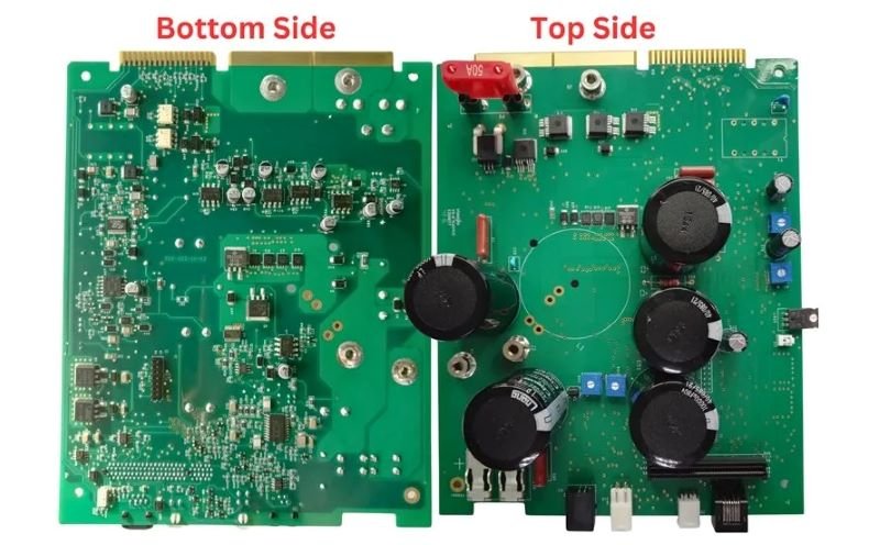
Double-Sided SMT Assembly Process
Double-sided SMT assembly takes the process a step further by allowing components to be mounted on both sides of the PCB. This technique offers several advantages, such as increased component density, improved functionality, and reduced PCB size.
The double-sided SMT assembly process involves the following steps:
1. PCB Design
The first step in double-sided SMT assembly is designing the PCB. The design must take into consideration the placement of components on both sides of the board. The designer must ensure that there is enough space for the components and that there are proper connections between the two sides.
2. Solder Paste Application
Once the PCB design is finalized, solder paste is applied to the pads on both sides of the board. This is typically done using a stencil, which ensures precise and consistent application of the solder paste.
3. Component Placement
After the solder paste is applied, the components are placed onto the pads on both sides of the PCB. This can be done manually or using automated pick-and-place machines. The components must be carefully aligned with the pads to ensure proper soldering.
4. Reflow Soldering
Once the components are placed, the PCB is passed through a reflow oven. The oven heats the board to a specific temperature, causing the solder paste to melt and form a strong bond between the components and the PCB. The reflow process is carefully controlled to ensure that the solder joints are properly formed.
5. Inspection and Testing
After the reflow process, the PCB is inspected to ensure that all components are properly soldered and that there are no defects. Various inspection techniques, such as automated optical inspection (AOI) or X-ray inspection, can be used to detect any potential issues. Once the inspection is complete, the PCB is tested to ensure its functionality.
The Benefits of Double-Sided SMT Assembly
Double-sided SMT assembly offers several benefits over traditional through-hole assembly and single-sided SMT assembly:
- Increased Component Density: Double-sided SMT assembly allows for a higher component density on the PCB. By utilizing both sides of the board, manufacturers can place more components in a smaller space, leading to more compact and efficient electronic devices. This is especially beneficial for devices with limited space, such as smartphones and wearables.
- Improved Functionality: With double-sided SMT assembly, manufacturers have more flexibility in designing complex electronic circuits. Components can be placed on both sides of the PCB, enabling the creation of intricate connections and advanced functionalities. This is particularly advantageous for devices that require multiple layers of circuitry, such as advanced medical devices or high-performance computers.
- Reduced PCB Size: Double-sided SMT assembly allows for smaller PCB sizes compared to through-hole assembly. By utilizing both sides of the board, manufacturers can minimize the overall footprint of the device, making it more compact and portable. This is especially important in industries where space is limited, such as aerospace or automotive.
- Cost Efficiency: Double-sided SMT assembly can be more cost-effective compared to through-hole assembly. The automated nature of the process reduces labor costs and increases production efficiency. Additionally, the smaller PCB size and increased component density can lead to cost savings in terms of materials and shipping.
- Enhanced Reliability: Double-sided SMT assembly offers improved reliability compared to through-hole assembly. The solder joints created during the reflow soldering process provide a strong and durable connection between the components and the PCB. This reduces the risk of loose connections or component failures, resulting in a more reliable electronic device.
Conclusion
In conclusion, Double-sided SMT assembly is a highly efficient and versatile method for electronic manufacturing. By utilizing both sides of the PCB, manufacturers can achieve higher component density, improved functionality, reduced PCB size, cost efficiency, and enhanced reliability. This technique plays a crucial role in the production of various electronic devices, from consumer electronics to advanced medical equipment. As technology continues to advance, double-sided SMT assembly will likely remain a key process in the electronics industry.