High Density Interconnect(HDI) Printed Circuit Boards
When it comes to PCB prototyping, there’s a spectrum of options available in the market, ranging from simple single-sided boards to intricate multi-layer ones. Basic prototypes typically feature copper tracks on just one surface, known as single-sided PCBs. However, for more complex designs, High Density Interconnect (HDI) PCBs are essential. These boards pack in more wiring per unit area compared to traditional PCBs and provide thinner spaces, smaller vias, and denser connection pads.
An HDI (High Density Interconnect) PCB is designed to have a higher density of components and interconnections than traditional PCBs. HDI PCBs are used in a wide range of electronic devices, including smartphones, tablets, laptops, and medical equipment. Let’s explore the definition of HDI PCB!
What is an HDI PCB?
HDI PCBs, or High-Density Interconnect PCBs, are a type of printed circuit board that offer increased functionality and miniaturization compared to traditional PCBs. HDI PCBs are designed to handle high-density components and complex circuitry which makes them ideal for use in modern electronic devices. HDI PCBs are characterized by their smaller size, higher component density and finer traces and spaces. They are designed to accommodate more complex circuitry in a smaller form factor and allows for the miniaturization of electronic devices.
There are several types of HDI PCBs, including 1+N+1, 2+N+2, and 3+N+3, which refer to the number of layers and the number of microvias used in the PCB. The specific design and configuration of an HDI PCB depend on the requirements of the electronic device it will be used in.
HDI PCBs offer better thermal management compared to traditional PCBs. The smaller size and increased component density of HDI PCBs result in reduced heat dissipation, which can help prevent overheating and improve the overall reliability and lifespan of the electronic device.
Structure of Different HDI PCBs
High-Density Interconnect (HDI) printed circuit boards (PCBs) are designed to have a higher circuit density and smaller form factor compared to traditional PCBs. The structure of HDI PCBs can vary depending on the specific design requirements and technology used. Here are three common types of HDI PCB structures:
1+N+1 HDI PCB Structure
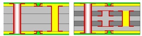
The 1+N+1 HDI PCB structure consists of a single high-density layer surrounded by one build-up layer on each side. This structure allows for increased routing density and smaller via sizes. It is suitable for applications that require moderate layer count and complexity.
2+N+2 HDI PCB Structure
The 2+N+2 HDI PCB structure features two high-density layers with two build-up layers on each side. This structure provides even higher routing density and allows for more complex designs. It is commonly used in advanced electronic devices that require a higher level of circuit integration.
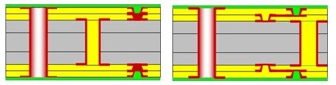
3+N+3 HDI PCB Structure
The 3+N+3 HDI PCB structure is the most complex among the three. It consists of three high-density layers with three build-up layers on each side. This structure offers the highest routing density and enables the most intricate circuit designs. It is often used in cutting-edge electronic devices that demand the utmost miniaturization and performance
Benefits of HDI Printed Circuit Boards
Let’s explore some benefits of HDI PCBs and why they are becoming increasingly popular in the electronics industry:
- Increased Component Density: HDI technology allows for the placement of smaller components and the routing of finer traces, resulting in a more compact design. With HDI PCBs, designers can achieve a higher level of integration, fitting more functionality into a smaller form factor.
- Improved Signal Integrity: HDI PCBs offer improved signal integrity compared to traditional PCBs. The shorter and more direct signal paths in HDI PCBs reduce the chances of signal loss or cross-talk between traces. Additionally, the use of microvias and buried vias in HDI PCBs helps minimize the impedance mismatch, ensuring reliable signal transmission.
- Enhanced Electrical Performance: The use of advanced materials and manufacturing techniques allows for better control over impedance, capacitance, and other electrical parameters. This enables designers to meet strict performance requirements and ensures optimal functionality of the electronic device. Whether it’s reducing power consumption, improving signal integrity or achieving higher data transfer rates, HDI PCBs can help deliver superior electrical performance.
- Increased Reliability: HDI PCBs are designed to improve reliability by reducing the number of interconnects and minimizing the risk of failure. The use of microvias and buried vias in HDI PCBs eliminates the need for through-hole vias, which are potential points of failure. The smaller vias also reduce the thermal stress on the PCB, improving its overall durability. Additionally, the compact design of HDI PCBs reduces the risk of mechanical failures, such as solder joint cracks or broken traces, during operation or transportation.
- Design Flexibility: HDI PCBs offer greater design flexibility compared to traditional PCBs. The smaller size and higher component density allow for more creative and innovative designs. HDI technology enables the use of multiple layers, blind vias, and buried vias, giving designers more freedom in routing and interconnect options. This flexibility not only improves the overall performance of the electronic device but also simplifies the assembly process, reducing manufacturing costs and time-to-market.
Common Usage of HDI PCBs
HDI (High Density Interconnect) PCBs find widespread usage across various industries due to their compactness, high performance, and versatility. Some common applications include:
- Consumer Electronics: HDI PCBs are extensively used in consumer electronics such as smartphones, tablets, laptops, and wearable devices. Their compact size and high wiring density allow for the integration of numerous components in small form factors, contributing to sleek designs and improved functionality.
- Communications: In the telecommunications industry, HDI PCBs play a crucial role in networking equipment, routers, switches, and base stations. Their high-speed signal transmission capabilities and reduced signal loss make them suitable for handling complex communication protocols.
- Automotive: HDI PCBs are increasingly employed in automotive applications, including infotainment systems, GPS navigation, driver assistance systems, and engine control units. They offer reliability in harsh operating environments, compactness for space-constrained designs, and the ability to support advanced features in modern vehicles.
- Medical Devices: Medical equipment often requires compact and lightweight designs without compromising on performance and reliability. HDI PCBs are used in devices such as medical imaging systems, patient monitoring devices, diagnostic equipment, and implantable medical devices, where high precision and signal integrity are essential.
- Aerospace and Defense: In aerospace and defense applications, where reliability and performance are critical, HDI PCBs are used in radar systems, avionics, missile guidance systems, and satellite communication systems. They provide high-density routing for complex electronic systems while meeting stringent quality and reliability standards.
- Industrial Automation: Industrial automation systems rely on HDI PCBs for their control units, sensors, actuators, and data acquisition modules. The compact size and high reliability of HDI PCBs enable efficient automation processes in manufacturing plants, robotics, and machinery.
Different Types of Vias in HDI PCBs
Vias are an essential component of any PCB, including HDI PCBs. They are used to create connections between different layers of the board, allowing for the transfer of electrical signals and power. Vias are essentially small holes drilled into the PCB, which are then plated with conductive material to establish a connection.
HDI PCBs typically utilize several different types of vias, each with its own unique characteristics and advantages. Let’s take a closer look at some of the most common types:
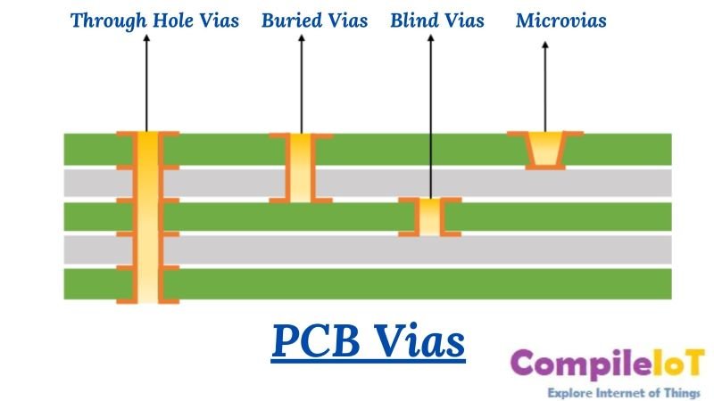
1. Through Vias
Through vias, as the name suggests, are vias that span through the entire thickness of the PCB, connecting all the layers together. These vias are commonly used to establish connections between the surface-mounted components and the inner layers of the board. Through vias are typically drilled using mechanical or laser drilling techniques and are plated with conductive material to ensure a reliable connection.
2. Blind Vias
Blind vias are vias that connect the outermost layer of the PCB to one or more inner layers, but do not span through the entire thickness of the board. These vias are drilled from the surface of the PCB and only go partway through, stopping at a specific layer. Blind vias are commonly used in HDI PCBs to reduce the number of layers required, allowing for a more compact design.
3. Buried Vias
Buried vias are similar to blind vias in that they do not span through the entire thickness of the PCB. However, instead of terminating at an outer layer, buried vias connect two or more inner layers of the board. These vias are drilled from within the PCB, and their presence is not visible from the outer layers. Buried vias are often used in HDI PCBs to further increase the density of connections without adding additional layers.
4. Microvias
Microvias are a specialized type of via that is significantly smaller in size compared to traditional vias. These vias are typically less than 150 micrometers in diameter and are used to establish connections between adjacent layers in the PCB.
Microvias can be further classified into two types: stacked microvias and staggered microvias.
Stacked microvias are vias that connect multiple layers of the PCB in a stacked configuration. They are drilled one on top of the other, allowing for high-density interconnections. Staggered microvias, on the other hand, are vias that connect adjacent layers in a staggered pattern, providing additional routing flexibility.
HDI vs Standard PCBs – What’s the Difference?
HDI (High Density Interconnect) PCBs and standard PCBs differ significantly in terms of their design, construction, and application. Here are the key differences between the two:
Wiring Density:
- HDI PCBs: HDI PCBs are designed to have a much higher wiring density compared to standard PCBs. They achieve this through advanced techniques such as microvias, buried vias, and sequential lamination, allowing for more interconnections in a smaller area.
- Standard PCBs: Standard PCBs typically have lower wiring densities and rely on through-hole vias for interconnections between layers.
Via Types:
- HDI PCBs: HDI PCBs utilize various types of vias, including microvias, blind vias, buried vias, and filled vias, to achieve high routing densities and optimize signal integrity.
- Standard PCBs: Standard PCBs predominantly use through-hole vias for interconnections, which can limit routing density and increase signal distortion, especially in complex designs.
Layer Count:
- HDI PCBs: HDI PCBs often have higher layer counts compared to standard PCBs, allowing for more complex and compact designs. They can incorporate multiple layers of high-density interconnects to accommodate densely packed components and intricate routing requirements.
- Standard PCBs: Standard PCBs typically have fewer layers, which may limit their ability to accommodate complex designs with high routing densities.
Size and Weight:
- HDI PCBs: HDI PCBs are typically smaller and lighter compared to standard PCBs due to their higher wiring densities and compact designs. This makes them well-suited for applications where space and weight are critical factors.
- Standard PCBs: Standard PCBs may be larger and heavier, especially in designs that require multiple boards to achieve the same functionality as a single HDI PCB.
Cost:
- HDI PCBs: HDI PCBs tend to be more expensive to manufacture compared to standard PCBs due to the use of advanced materials and processes required to achieve high wiring densities and complex designs.
- Standard PCBs: Standard PCBs are generally more cost-effective to manufacture, making them a preferred choice for simpler designs or applications where cost is a primary concern.
Conclusion
In summary, High Density Interconnect (HDI) PCBs revolutionize electronics with increased functionality and miniaturization. Characterized by smaller size, higher component density, and advanced thermal management, they are vital for modern devices. HDI PCBs offer superior signal integrity and reliability, shaping the future of electronic innovation