Flip Chip – A detailed Guide
What is a Flip Chip?
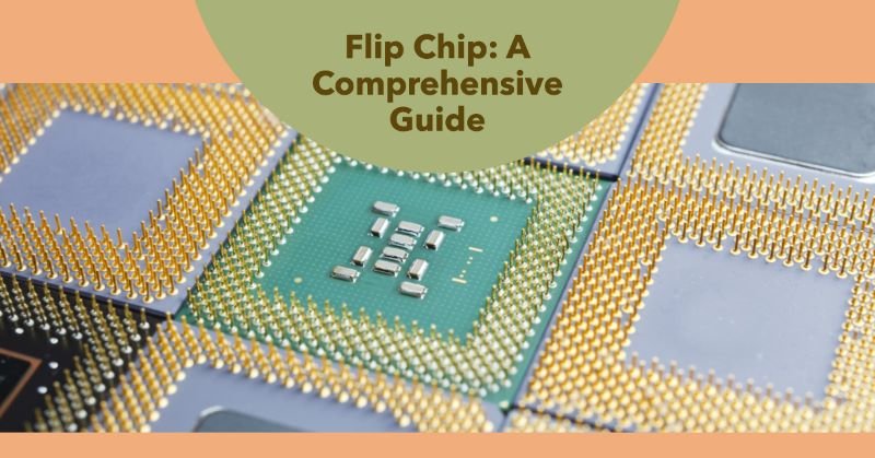
A flip chip is a type of semiconductor packaging technology that allows for the direct electrical connection between the integrated circuit (IC) and the substrate or printed circuit board (PCB). In a flip chip package, the IC is flipped upside down and its solder bumps are directly bonded to the corresponding contact pads on the substrate or PCB. This method of packaging offers several advantages over traditional wire bonding techniques, such as improved electrical performance, higher density, and better thermal management.
Common Flip Chip Packages
There are several types of flip chip packages available in the market, each with its own unique characteristics and applications. Here are some of the most common flip chip packages:
1. Flip Chip Ball Grid Array (FCBGA)
The Flip Chip Ball Grid Array (FCBGA) package is one of the most widely used flip chip packages. It features an array of solder balls on the bottom side of the IC, which are used to make the electrical connections with the PCB. FCBGA packages are known for their high density and excellent thermal performance, making them suitable for a wide range of applications, including microprocessors, graphics processors and memory modules.
2. Flip Chip Quad Flat No-Lead (FCQFN)
The Flip Chip Quad Flat No-Lead (FCQFN) package is a variation of the traditional Quad Flat No-Lead (QFN) package. It eliminates the need for wire bonding by directly connecting the IC to the PCB using solder bumps. FCQFN packages offer a smaller form factor and improved electrical performance compared to their wire-bonded counterparts. They are commonly used in applications where space is limited, such as mobile devices, consumer electronics and automotive systems.
3. Flip Chip Small Outline Package (FCSOP)
The Flip Chip Small Outline Package (FCSOP) is a flip chip version of the popular Small Outline Package (SOP). It features solder bumps on the bottom side of the IC, which are used for electrical connections. FCSOP packages offer a smaller footprint and better electrical performance compared to traditional wire-bonded SOP packages. They are commonly used in applications where size and performance are critical, such as portable electronics, IoT devices and medical implants.
4. Flip Chip Plastic Ball Grid Array (FCPBGA)
The Flip Chip Plastic Ball Grid Array (FCPBGA) package is similar to the FCBGA package but uses a plastic encapsulation instead of ceramic. This makes FCPBGA packages more cost-effective and suitable for high-volume production. They are commonly used in a wide range of applications, including networking equipment, telecommunications devices and automotive electronics.
5. Flip Chip Chip Scale Package (FCCSP)
The Flip Chip Chip Scale Package (FCCSP) is a compact flip chip package that offers a small form factor and high density. It features solder bumps on the bottom side of the IC, allowing for direct electrical connections with the PCB. FCCSP packages are commonly used in applications where space is limited, such as mobile devices, wearables and IoT sensors.
The Flip Chip Process
The flip chip process involves several key steps:
- Die preparation: The semiconductor die is thinned down to a specified thickness and then cleaned to remove any contaminants.
- Bump formation: Small solder bumps or copper pillars are formed on the contact pads of the die. These bumps serve as the electrical connections between the die and the substrate.
- Wafer dicing: The wafer containing multiple die is diced into individual units.
- Die attach: The die is carefully placed onto the substrate or circuit board, aligning the solder bumps with the corresponding contact pads.
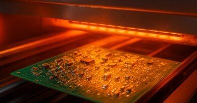
- Reflow: The assembly is heated to a specific temperature to melt the solder bumps, creating a reliable and permanent connection between the die and substrate.
- Underfill: A liquid epoxy is dispensed around the solder bumps to provide mechanical support and protect the connections from mechanical stress and moisture.
Why Use a Flip Chip BGA?
Flip chip ball grid array (BGA) is a specific type of flip chip packaging that offers several advantages over traditional packaging methods. Here are some reasons why flip chip BGAs are commonly used:
- Higher performance: Flip chip technology allows for shorter electrical connections, reducing signal delays and improving overall performance. The direct connection between the chip and the substrate also enables higher data transfer speeds.
- Increased miniaturization: Flip chip BGAs have a smaller footprint compared to other packaging methods, making them ideal for applications where space is limited. The absence of wire bonds also allows for more compact designs.
- Better thermal management: The direct attachment of the chip to the substrate enhances heat dissipation, improving the overall thermal performance of the integrated circuit. This is particularly beneficial for high-power applications that generate a significant amount of heat.
- Improved electrical and mechanical reliability: Flip chip BGAs offer better electrical and mechanical connections compared to wire bonding. The solder bumps provide a more reliable and robust connection, reducing the risk of failures due to wire bond lifting or breaking.
- Cost-effectiveness: While flip chip technology may have higher upfront costs due to the complexity of the manufacturing process, it can lead to cost savings in the long run. The smaller size and improved performance of flip chip BGAs can result in lower material and assembly costs, as well as reduced power consumption.
Challenges with Flip Chip BGA
Despite the numerous benefits of flip chip BGAs, there are also some challenges associated with this packaging technology. Here are a few common challenges:
- High precision manufacturing: Flip chip BGAs require precise alignment of the solder bumps with the corresponding pads on the substrate. Any misalignment or defects in the solder joints can lead to electrical failures or reduced reliability.
- Thermal management: While flip chip BGAs offer better thermal performance overall, they can also present challenges in terms of managing heat dissipation. The compact design and direct attachment of the chip to the substrate can result in localized hotspots, requiring careful thermal design and heat sink solutions.
- Testing and repair: The direct connection between the chip and the substrate makes it more difficult to test and repair flip chip BGAs compared to other packaging methods. Specialized equipment and techniques are required to access and diagnose potential issues.
- Reliability under mechanical stress: Flip chip BGAs may be more susceptible to mechanical stress, such as vibrations or shocks, due to their direct attachment to the substrate. This can potentially lead to solder joint fatigue or failures over time.
- Cost and complexity: Flip chip technology can be more complex and expensive compared to traditional packaging methods. The manufacturing process involves additional steps, such as bumping and underfilling, which can increase the overall cost of production.
Conclusion
In conclusion, Flip chip packaging technology offers numerous advantages over traditional wire bonding techniques, including improved electrical performance, higher density and better thermal management. There are several types of flip chip packages available in the market, each with its own unique characteristics and applications. Whether it’s the high density of FCBGA, the small form factor of FCQFN or the cost-effectiveness of FCPBGA, flip chip packages have become an integral part of modern semiconductor packaging.