BGA in PCB Assembly: Types, benefits, and inspection techniques
In this blog post, we will explore the different types of BGAs, the benefits they offer, and the inspection techniques used to ensure their quality. Whether you are new to PCB assembly or looking to expand your knowledge, this article will provide you with valuable insights into the world of BGA in PCB assembly.
What is BGA?
BGA is a type of surface mount technology (SMT) that is used to mount integrated circuits onto a printed circuit board (PCB). Unlike traditional through-hole components, BGA packages do not have leads that go through the PCB. Instead, they have small solder balls on the bottom side of the package, which are used to make electrical connections with the PCB.
BGA packages come in various sizes, ranging from a few millimeters to several centimeters. The number of solder balls on a BGA package can also vary, depending on the complexity of the integrated circuit.
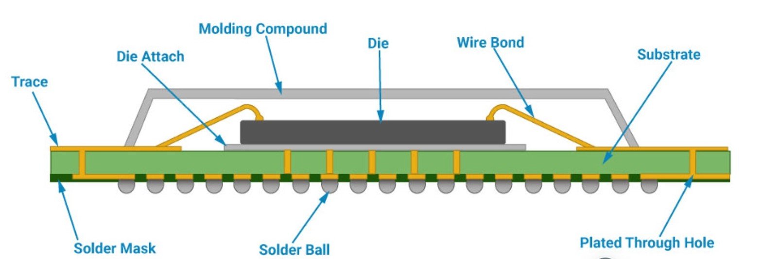
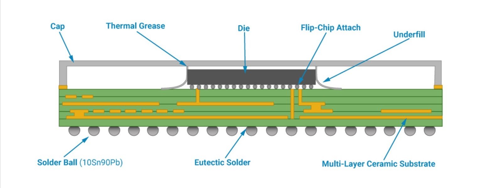
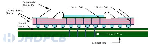
Figure (1) and Figure (2) show how BGA devices are made. Figure (1) demonstrates how the BGA chip is attached to the board using tiny wires, while Figure (2) shows how it’s connected using a different method called flip-chip.
In both cases, the connections from the chip to the board are made using metal lines on the board. BGA packages have more connection points than other types of packages, which helps them handle more data.
Plus, because the connections are shorter in BGAs, they work faster, especially when transferring lots of data.
What is BGA POP?
BGA POP, or Package on Package, is an advanced packaging technology that combines two or more IC packages together to achieve higher functionality and performance. It involves stacking multiple IC packages vertically on top of each other, with the bottom package acting as the base and the top package serving as an additional layer.
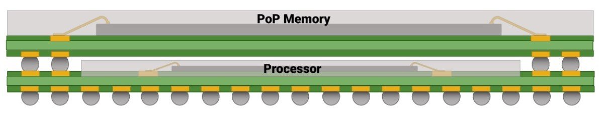
The primary benefit of BGA POP is the ability to integrate multiple functions into a single module, thereby reducing the overall size of the electronic device. For example, in a mobile phone, the base package may contain the main processor, while the top package can house the memory chips or other peripheral components. This compact design not only saves space but also improves signal integrity and reduces power consumption.
How does BGA work?
The process of mounting a BGA package onto a PCB involves several steps. First, solder paste is applied to the pads on the PCB. Then, the BGA package is carefully placed on top of the solder paste, aligning the solder balls with the corresponding pads on the PCB.
Next, the PCB with the BGA package is heated in a reflow oven. The heat melts the solder paste, creating a strong bond between the BGA package and the PCB. As the solder cools down, it solidifies and forms a reliable electrical connection between the BGA package and the PCB.
The Benefits of BGA in PCB Assembly
BGA offers several advantages over other types of integrated circuit packaging, making it a popular choice in PCB assembly:
1. Space-saving design:
BGA packages have a smaller footprint compared to through-hole components, allowing for higher component density on the PCB. This is especially beneficial in applications where space is limited, such as mobile devices and compact electronics.
2. Improved thermal performance:
The solder balls on BGA packages provide a larger surface area for heat dissipation compared to traditional leads. This allows for better thermal performance and helps to prevent overheating of the integrated circuit.
3. Enhanced electrical performance:
The shorter electrical paths in BGA packages result in lower inductance and capacitance, leading to improved signal integrity and faster data transfer rates. This makes BGA packages ideal for high-speed applications, such as microprocessors and memory modules.
4. Better reliability:
The solder balls on BGA packages create a strong mechanical bond with the PCB, making them more resistant to mechanical stress and vibration. This enhances the overall reliability of the PCB assembly.
Types of BGA Packages
There are several types of BGA packages available, each with its own characteristics and applications. Let’s take a closer look at some of the most common types:
1. Ceramic BGA (CBGA)
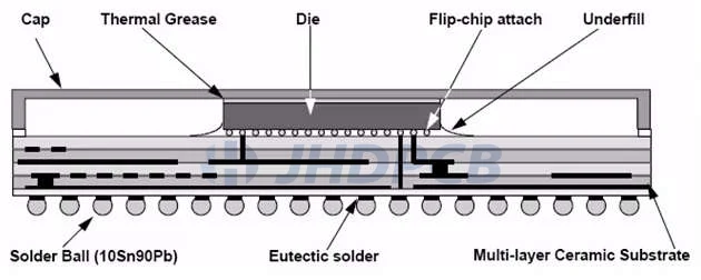
Ceramic BGA packages are known for their excellent thermal and electrical performance. They are typically used in high-frequency applications, such as microprocessors and high-speed memory modules. The ceramic material used in these packages provides better heat dissipation compared to other materials, making them ideal for devices that generate a lot of heat.
CBGA packages come in different sizes and configurations, ranging from small packages with a few dozen solder balls to larger ones with several hundred balls.
2. Plastic BGA (PBGA)
Plastic BGA packages are widely used in consumer electronics and other cost-sensitive applications. They are made of a plastic material, which makes them less expensive to produce compared to ceramic packages. PBGA packages are available in various sizes and ball counts, making them suitable for a wide range of devices.
While PBGA packages may not offer the same level of thermal and electrical performance as CBGA packages, they are still capable of meeting the requirements of many applications.
3. Flip Chip BGA (FCBGA)
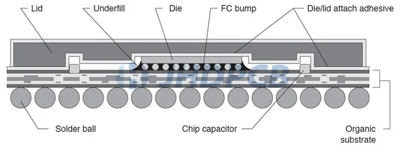
Flip Chip BGA packages are a variation of the traditional BGA technology. In FCBGA packages, the IC is flipped upside down and directly bonded to the substrate using solder bumps or copper pillars. This allows for shorter electrical connections and improved electrical performance.
FCBGA packages are commonly used in high-performance applications where signal integrity and electrical performance are critical, such as graphics processors and high-speed communication devices.
4. Micro BGA (µBGA)
Micro BGA packages are smaller versions of the traditional BGA packages. They are designed for space-constrained applications where size is a critical factor. µBGA packages typically have a smaller number of solder balls and a smaller footprint compared to other BGA packages.
Despite their small size, µBGA packages still offer good electrical performance and are commonly used in mobile devices, such as smartphones and tablets.
Inspection Techniques for BGAs
Ensuring the quality and reliability of BGAs is crucial for the success of any PCB assembly. Here are some commonly used inspection techniques:
1. X-ray Inspection
X-ray inspection is a non-destructive technique that allows for the detection of defects such as voids, cracks, and misalignment in the solder joints of BGAs. It provides a clear image of the internal structure of the BGA, enabling inspectors to identify any potential issues that may affect its performance.
2. Optical Inspection
Optical inspection involves the use of a microscope or a camera to visually inspect the solder joints of BGAs. This technique is effective in detecting surface defects such as solder bridges, insufficient solder, or misalignment. It is a cost-effective and efficient method for inspecting BGAs during the assembly process.
3. Automated Optical Inspection (AOI)
AOI is a computer-based inspection technique that uses advanced algorithms to analyze images of BGAs and identify any defects or anomalies. It offers a fast and accurate way to inspect BGAs, ensuring that they meet the required quality standards. AOI can detect defects such as missing solder balls, tombstoning, and solder bridging.
The Process of Soldering BGA to a PCB
Ball Grid Array (BGA) is a type of surface mount packaging technology commonly used in electronic devices. It offers many advantages such as higher pin density, improved electrical performance, and better thermal dissipation. Soldering a BGA to a PCB requires careful attention to detail and precise techniques. In this article, we will explore the step-by-step process of soldering a BGA to a PCB.
1. PCB Preparation
The first step in soldering a BGA to a PCB is to prepare the PCB itself. This involves cleaning the PCB to remove any dust, dirt, or debris that may interfere with the soldering process. It is important to ensure that the PCB surface is clean and free from any contaminants.
Additionally, the PCB should be inspected for any defects or damage that could affect the soldering process. Any issues should be addressed and resolved before proceeding with the soldering of the BGA.
2. Applying Solder Paste
Once the PCB is prepared, the next step is to apply solder paste to the pads where the BGA will be soldered. Solder paste is a mixture of solder alloy particles and flux, which helps facilitate the soldering process.
The solder paste is applied using a stencil, which ensures precise and consistent application. The stencil is aligned with the PCB pads, and the solder paste is spread over the stencil and onto the pads using a squeegee or a similar tool. The excess solder paste is then removed, leaving a uniform layer on the pads.
3. Placing the BGA
Once the solder paste is applied, the BGA is carefully placed onto the PCB, aligning the balls on the BGA with the corresponding pads on the PCB. This step requires precision and accuracy to ensure proper alignment.
Special care should be taken to avoid any damage to the BGA or the PCB during the placement process. It is recommended to use specialized tools or equipment, such as a pick-and-place machine, to ensure accurate placement.
4. Reflow Soldering
After the BGA is placed on the PCB, the soldering process begins. Reflow soldering is the most common method used to solder BGAs to PCBs. It involves subjecting the PCB to a controlled heating and cooling process to melt the solder paste and form a reliable solder joint.
The PCB with the BGA is placed in a reflow oven or a similar heating device. The temperature is carefully controlled to ensure that the solder paste melts and flows, creating a strong bond between the BGA and the PCB pads.
During the reflow process, the solder paste undergoes a phase change from a solid to a liquid state, allowing the solder balls on the BGA to connect with the corresponding pads on the PCB. The temperature is then gradually reduced, causing the solder to solidify and form a permanent bond.
5. Inspection and Testing
Once the soldering process is complete, the PCB with the soldered BGA is inspected and tested to ensure the quality and reliability of the solder joints. This step is crucial to identify any defects or issues that may have occurred during the soldering process.
Visual inspection is performed to check for any visible defects such as solder bridges, insufficient solder, or misalignment. Additionally, various testing methods such as X-ray inspection, thermal testing, and electrical testing are used to verify the integrity of the solder joints and the functionality of the BGA.