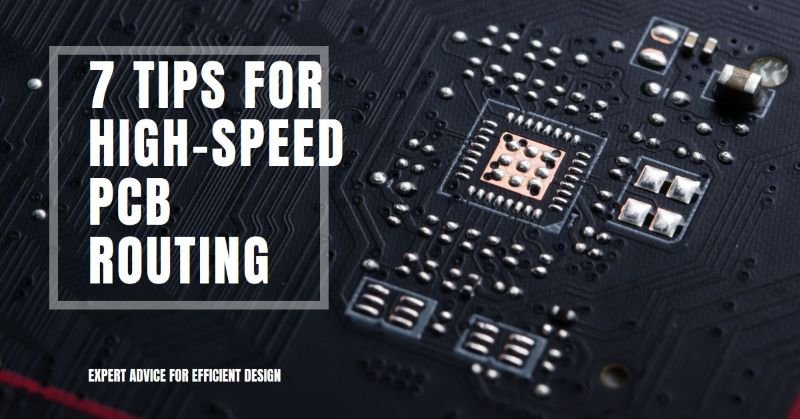
7 Tips for high speed PCB routing design
In high-speed PCB routing design, there are several factors to consider in order to ensure optimal performance and reliability. Whether you are designing a PCB for a high-speed digital application or a high-frequency analog circuit, following these 7 tips will help you achieve the best results.
What is a high speed PCB design?
High-speed PCB design refers to the process of creating printed circuit boards (PCBs) that are optimized for the transmission of high-frequency signals. In today’s fast-paced technological world, where data transfer rates and signal integrity are crucial, high-speed PCB design plays a vital role in the development of electronic devices.
The Importance of High-Speed PCB Design
With the increasing demand for faster and more efficient electronic devices, the need for high-speed PCB design has become paramount. Whether it’s in consumer electronics, telecommunications, or industrial applications, high-speed PCBs are essential for ensuring reliable and accurate signal transmission.
High-speed PCBs are designed to minimize the effects of signal degradation, such as noise and interference, that can occur at high frequencies. These boards are engineered to have controlled impedance, reduced crosstalk, and minimal signal loss, allowing for the efficient transfer of data.
The Design Process for High-Speed PCBs
The design process for high-speed PCBs typically involves the following steps:
1. Requirements Gathering:
The first step is to gather the requirements and specifications for the PCB. This includes understanding the desired data transfer rates, the type of components to be used, and any specific design constraints.
2. Schematic Design:
Once the requirements are gathered, the next step is to create a schematic diagram of the PCB. This involves placing and connecting the components, defining the signal paths, and ensuring proper power distribution.
3. PCB Layout:
After the schematic design is complete, the PCB layout process begins. This involves translating the schematic into a physical layout, including the placement of components, routing of traces, and consideration of signal integrity and thermal management.
4. Design Verification:
Once the PCB layout is complete, it undergoes a thorough verification process to ensure that it meets the design requirements. This includes checking for signal integrity issues, verifying impedance matching, and performing thermal analysis.
5. Prototyping and Testing:
After the design is verified, a prototype PCB is manufactured and tested to validate its performance. This involves testing for signal integrity, power integrity, EMI/EMC compliance, and thermal performance.
Tips for design high speed PCB routing design
Let’s explore seven tips for high-speed PCB routing design that will help you achieve optimal performance:
1. Plan your layout carefully
Before starting the routing process, it is important to plan your layout carefully. Consider the placement of critical components, such as high-speed ICs, connectors, and power supplies. Make sure to keep signal paths as short as possible and minimize the number of vias and trace crossovers. This will help reduce signal degradation and improve overall signal integrity.
2. Use proper layer stack-up
Choosing the right layer stack-up is crucial for high-speed PCB routing design. Use a stack-up that provides good impedance control and minimizes signal reflections. Consider using controlled impedance traces for high-speed signals to maintain signal integrity. Also, ensure that the power and ground planes are properly placed to provide a low impedance return path for high-frequency signals.
3. Minimize trace length and impedance mismatches
High-speed signals are prone to reflection and signal degradation. Minimize trace length to reduce signal propagation delay and avoid impedance mismatches. Use controlled impedance traces to match the characteristic impedance of the transmission lines. This will help minimize signal reflections and ensure proper signal transmission.
4. Use differential pairs for high-speed signals
For high-speed signals, it is recommended to use differential pairs. This technique helps to improve signal integrity and reduce electromagnetic interference (EMI). Keep the differential traces as close together as possible and maintain a consistent spacing throughout the routing. This will help minimize crosstalk and ensure proper signal transmission.
5. Pay attention to power and ground planes
Power and ground planes play a crucial role in high-speed PCB routing design. Ensure that the power and ground planes are properly placed and provide a low impedance return path for high-frequency signals. Use multiple vias to connect the power and ground planes to minimize impedance and reduce noise. Also, avoid splitting power and ground planes, as this can lead to increased EMI.
6. Use proper decoupling and bypass capacitors
Decoupling and bypass capacitors are essential for high-speed PCB routing design. Place decoupling capacitors as close as possible to the power pins of ICs to provide a local energy source and reduce noise. Use bypass capacitors to filter out high-frequency noise and ensure stable power supply. Pay attention to the value and placement of these capacitors to achieve optimal performance.
7. Perform signal integrity analysis
After completing the routing process, it is important to perform signal integrity analysis to ensure that the design meets the required specifications. Use simulation tools to analyze signal integrity, identify potential issues such as signal reflections, crosstalk, and impedance mismatches, and make necessary adjustments to the design. This will help optimize the performance and reliability of the PCB.
Conclusion
In conclusion, High-speed PCB routing design requires careful planning and attention to detail. By following these 7 tips, you can ensure optimal performance and reliability of your PCB design. Remember to plan your layout carefully, use proper layer stack-up, minimize trace length and impedance mismatches, use differential pairs for high-speed signals, pay attention to power and ground planes, use proper decoupling and bypass capacitors, and perform signal integrity analysis. By implementing these best practices, you can achieve high-speed PCB designs that meet the demanding requirements of today’s technology.