A Beginner’s Guide to Multisim PCB
If you are new to the world of electronics and printed circuit board (PCB) design, you may have heard about Multisim PCB. Multisim is a powerful software tool that allows engineers, students and hobbyists to design and simulate electronic circuits. In this beginner’s guide, we will explore the basics of Multisim PCB, its features, and how you can get started with designing your own PCBs.
Understanding Multisim PCB
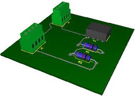
Multisim PCB, also known as Ultiboard, is a software package developed by National Instruments for designing printed circuit boards. It is part of the broader Multisim suite, which also includes circuit simulation capabilities. Multisim PCB provides a user-friendly interface for designing PCB layouts, creating schematics and preparing designs for manufacturing.
Differences Between Multisim PCB Design and Traditional PCB Design
When comparing Multisim PCB design with traditional PCB design methods, several key differences become apparent. Understanding these differences can help in determining which approach is best suited for a particular project or application.
Simulation and Testing Capabilities
With Multisim, users can simulate the behavior of electronic circuits, analyze performance and identify potential issues before moving to the physical prototyping stage. This can significantly reduce the time and resources required for iterative design and testing processes. In contrast, traditional PCB design often relies on building physical prototypes for testing, which can be more time-consuming and costly.
Additionally, Multisim PCB provides advanced simulation features such as interactive measurement instruments, virtual oscilloscopes and customizable analyses, allowing for in-depth evaluation of circuit performance. These capabilities are not readily available in traditional PCB design processes, giving Multisim users a distinct advantage in refining their designs and ensuring optimal functionality.
Integration with Circuit Design
Users can seamlessly transition from designing the circuit schematic to simulating its behavior within the same software environment. This integration streamlines the design process and facilitates a more cohesive workflow, as changes made in the schematic are immediately reflected in the simulation. In traditional PCB design, the circuit design and simulation phases are often more disjointed, requiring the use of separate tools and workflows for each stage.
Collaboration and Documentation
Multisim PCB provides robust features for sharing designs, generating reports and documenting the entire design process. Users can collaborate on projects more effectively by sharing design files, simulation results and comprehensive design documentation within the software. This collaborative environment fosters teamwork and knowledge sharing, which can be invaluable in complex design projects or educational settings.
Steps Involved in Schematics Creation in Multisim PCB
Creating schematics in Multisim PCB is an essential part of the design process for electronic circuits. Now, we will walk through the steps involved in creating schematics in Multisim PCB, from the initial setup to the final simulation and analysis.
1 – Begin with Multisim Software
The first step in creating schematics in Multisim PCB is to launch the software and create a new project. Upon opening the software, you will be prompted to start a new design. Select the appropriate options for your project, such as the type of circuit you are designing and the components you plan to use.
Once the project is created, you will be presented with a blank canvas where you can begin laying out your circuit. This is where the real magic happens, as you have the freedom to design and test various circuit configurations without the need for physical components.
2 – Selection of Components in Multisim PCB Software
After setting up the project, the next step is to select the components you want to include in your circuit. Multisim PCB offers a vast library of components ranging from basic resistors and capacitors to complex integrated circuits and microcontrollers. You can either search for specific components or browse through the categories to find the ones you need.
Once you have located the components, simply drag and drop them onto the canvas. You can then arrange and connect the components as per your circuit design requirements. Multisim PCB provides a user-friendly interface for component selection and placement, making it easy to build your circuit virtually.
3 – Wiring of the Components
With the components in place, the next step is to wire them together to form the desired circuit. Multisim PCB offers a range of tools for drawing wires and connecting the components. You can easily establish connections between different components by clicking on the connection points and dragging the wires to the respective connection points on other components.
It’s important to ensure that the connections are made accurately to reflect the intended circuit design. Multisim PCB provides features such as snap-to-grid and alignment guides to help you create neat and organized circuit diagrams.
4 – Addition of Power Sources
Every electronic circuit requires power to operate, and in Multisim PCB, you can easily add power sources to your circuit. Whether it’s a simple DC power supply or a more complex waveform generator, Multisim PCB offers a variety of power sources to suit your circuit’s needs.
By adding the appropriate power sources and configuring their properties, you can ensure that your circuit is powered correctly during simulation. This step is crucial in accurately representing the behavior of the circuit under different operating conditions.
5 – Simulation of the Circuit
Once the components, connections, and power sources are set up, it’s time to simulate the circuit. Multisim PCB’s simulation capabilities allow you to test the functionality of your circuit and observe its behavior under various conditions. You can apply input signals, analyze output responses, and troubleshoot any issues that may arise during simulation.
During the simulation, you can observe voltage and current levels at different points in the circuit, making it easier to identify potential problems or areas for improvement. Multisim PCB provides real-time feedback, allowing you to make iterative changes to the circuit design as needed.
6 – Results Analysis
After running the simulation, it’s essential to analyze the results to ensure that the circuit performs as intended. Multisim PCB offers tools for visualizing simulation data, such as oscilloscopes and graphs, which allow you to examine the circuit’s behavior in detail.
By carefully analyzing the simulation results, you can verify the functionality of the circuit and make informed decisions about any modifications or optimizations that may be required. This step is crucial in the design process, as it helps validate the circuit’s performance before moving on to the physical implementation.
7 – Iteration
Designing and simulating electronic circuits is often an iterative process, and Multisim PCB supports this approach by allowing you to make iterative changes to the circuit design based on simulation results. Whether it’s adjusting component values, refining connections, or experimenting with different configurations, Multisim PCB enables you to iterate on your design until you achieve the desired performance.
Why Simulating Circuits in Multisim Before PCB Layout are Important?
The process of simulating circuits in Multisim before PCB layout is of paramount importance. This practice offers a myriad of benefits that can significantly impact the overall success of a project. From error prevention and cost savings to performance optimization and improved collaboration, the advantages of simulating circuits in Multisim are undeniable.
Error Prevention
One of the key reasons for simulating circuits in Multisim before PCB layout is to prevent errors. By simulating the circuit design, engineers can identify and rectify potential issues or flaws in the design before it is translated into a physical PCB. This proactive approach helps in avoiding costly mistakes and rework, ultimately saving time and resources.
Cost Savings
Simulating circuits in Multisim can lead to significant cost savings in the long run. By detecting and addressing design flaws early in the process, the need for expensive redesigns or prototype iterations is minimized. This not only reduces material wastage but also optimizes the allocation of resources, resulting in cost-efficient project execution.
Time Efficiency
Time is of the essence in any design project, and simulating circuits in Multisim contributes to time efficiency. By uncovering and resolving potential issues at the simulation stage, engineers can streamline the overall design process. This, in turn, accelerates the development timeline, allowing for quicker iterations and faster time-to-market for the final product.
Performance Optimization
Simulating circuits in Multisim enables engineers to fine-tune and optimize the performance of the circuit. Through simulation, various parameters and configurations can be tested and adjusted to achieve the desired performance outcomes. This iterative process of optimization ultimately results in a more robust and efficient circuit design.
Design Validation
Before committing to the physical implementation of a circuit design, it is crucial to validate its functionality and performance. Multisim simulation provides a platform for thorough design validation, allowing engineers to verify the behavior of the circuit under different conditions and scenarios. This validation process instills confidence in the design before moving forward with the PCB layout.
Ease of Use
Multisim offers a user-friendly interface and intuitive tools for simulating circuits, making it accessible to both novice and experienced engineers. The ease of use of Multisim empowers designers to explore and experiment with different circuit configurations, fostering creativity and innovation in the design process.
Resource Efficiency
Simulating circuits in Multisim promotes resource efficiency by reducing the consumption of materials and components during the design phase. Through simulation, engineers can identify the most efficient component choices and configurations, optimizing the utilization of resources and minimizing waste.
Improved Collaboration
Collaboration is essential in complex design projects, and Multisim facilitates improved collaboration among team members. By simulating circuits in a virtual environment, engineers can easily share and discuss the design with colleagues, enabling seamless collaboration and knowledge exchange. This collaborative approach often leads to enhanced problem-solving and innovative solutions.
Common Issues Encountered in Multisim PCB Design
Designing a printed circuit board (PCB) using Multisim can be a rewarding experience, but it’s not without its challenges. Whether you’re a seasoned professional or a novice, encountering issues during the PCB design process is not uncommon. In this article, we’ll explore some of the common issues that arise during Multisim PCB design and provide practical solutions to fix them.
1. Component Placement and Routing
One of the most common issues encountered during Multisim PCB design is the placement of components and the routing of traces. Poor component placement can lead to signal interference, while improper routing can result in high impedance and signal distortion.
To fix these issues, it’s important to follow best practices for component placement and routing. Start by organizing components in a logical and systematic manner, considering factors such as signal flow, power distribution, and thermal management. When it comes to routing, ensure that traces are kept as short as possible, and that high-speed signals are properly impedance matched.
2. Power Integrity and Signal Integrity
Power integrity and signal integrity are critical aspects of PCB design, and issues in these areas can lead to malfunctions and performance degradation. Common problems include voltage drops, ground bounce, and electromagnetic interference (EMI).
To address power integrity issues, it’s essential to carefully plan power distribution, minimize voltage drops, and use decoupling capacitors to stabilize voltage levels. For signal integrity, consider factors such as trace length matching, controlled impedance routing, and proper grounding techniques to mitigate EMI and signal distortion.
3. Thermal Management
Thermal management is often overlooked but is a crucial aspect of PCB design, especially for high-power applications. Inadequate thermal dissipation can lead to overheating, component failure, and reduced lifespan of the PCB.
To tackle thermal issues, consider the placement of heat-generating components, use thermal vias to improve heat dissipation, and ensure proper airflow within the enclosure. Additionally, the selection of appropriate materials and the use of heat sinks can significantly improve the thermal performance of the PCB.
4. EMI and EMC Compliance
Electromagnetic interference (EMI) and electromagnetic compatibility (EMC) are major concerns in PCB design, particularly for products intended for commercial or industrial use. Failure to address EMI and EMC issues can result in failed compliance tests and costly redesigns.
To mitigate EMI and ensure EMC compliance, consider implementing shielding techniques, using ground planes effectively, and employing proper filtering and isolation methods. It’s also important to adhere to industry standards and regulations to ensure that the PCB design meets electromagnetic compatibility requirements.
5. Design for Manufacturability (DFM)
Design for manufacturability (DFM) issues can arise when the PCB design is not optimized for efficient and cost-effective manufacturing processes. Common DFM issues include excessive board complexity, inadequate clearances, and non-standard component footprints.
To address DFM issues, it’s crucial to collaborate closely with manufacturers and fabricators during the design phase. Consider simplifying the design where possible, adhering to standard PCB stackup configurations, and ensuring that component footprints and clearances meet manufacturing specifications. By optimizing the design for manufacturability, you can streamline the production process and minimize the risk of manufacturing-related issues.
6. Testing and Validation
Testing and validation are integral parts of the PCB design process, and issues in this area can lead to undetected faults and performance discrepancies. Common problems include inadequate test coverage, insufficient validation protocols, and reliance on simulation results without real-world verification.
To address testing and validation issues, it’s important to develop comprehensive test plans that cover functional, electrical, and environmental testing. Additionally, consider prototyping and conducting thorough validation tests to ensure that the PCB design meets performance requirements and reliability standards. Real-world validation is essential to uncovering potential issues that may not be evident in simulations alone.
Conclusion
In conclusion, Multisim PCB is a versatile and comprehensive tool for designing printed circuit boards. Its intuitive interface, seamless integration with circuit simulation, and support for manufacturing outputs make it an ideal choice for beginners and professionals alike. By following this beginner’s guide and leveraging the available resources, you can embark on your PCB design journey with confidence and proficiency.
