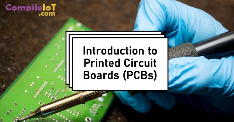
Introduction to Printed Circuit Boards (PCBs)
Printed Circuit Boards are the backbone of modern electronics, providing the necessary support and connectivity for electronic components to function together. Their compactness, reliability, and cost efficiency make them an essential component in a wide range of electronic devices. In this article, we will provide you with a comprehensive introduction to PCBs, explaining what they are, how they work, and their importance in modern technology.
What is a Printed Circuit Board (PCB)?
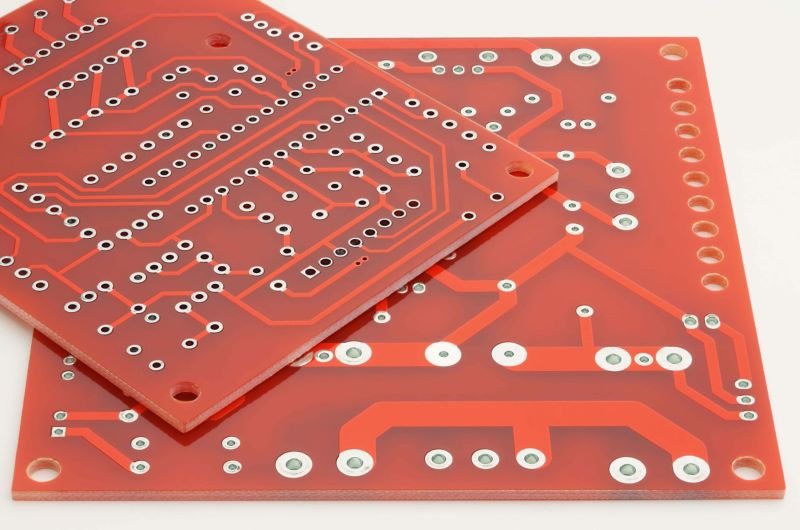
A Printed Circuit Board (PCB) is a flat board made of non-conductive material, usually fiberglass, that provides mechanical support and electrical connections for electronic components. It is used in almost all electronic devices, from smartphones and computers to home appliances and automotive systems. The main purpose of a PCB is to provide a platform for mounting and interconnecting various electronic components, such as resistors, capacitors, and integrated circuits, allowing them to communicate and work together to perform specific functions.
The Construction of a PCB – A typical PCB consists of a thin board made of non-conductive material, usually fiberglass or composite epoxy. On this board, a thin layer of conductive material, such as copper, is etched to create pathways called traces. These traces act as the interconnections between the different components on the board.
The components are then soldered onto the PCB, with their leads or terminals connected to the appropriate traces. This soldering process ensures a secure and reliable connection between the components and the PCB. A PCB is usually made of a non-conductive material, such as fiberglass or epoxy, with a thin layer of copper foil laminated onto it. The copper foil is etched to create pathways, also known as traces, that form the circuitry of the electronic device.
How Does a Printed Circuit Board (PCB) Work?
At its core, a PCB works by providing a network of pathways, called traces, that connect the various electronic components on the board. These traces are made of conductive material, usually copper, which allows the flow of electrical current between the components.
The design of a PCB is created using specialized software, which allows engineers to lay out the components and traces in an efficient and organized manner. Once the design is complete, it is sent to a manufacturer who uses a process called etching to remove the excess copper and create the desired traces.
After the etching process, the PCB is populated with the electronic components using soldering techniques. These components are carefully placed and soldered onto the board, ensuring proper electrical connections. Once all the components are in place, the PCB is tested to ensure its functionality before being integrated into the final product.
The Importance of Printed Circuit Boards (PCBs)
Printed Circuit Boards play a crucial role in the world of electronics and technology. Here are a few reasons why they are so important:
- Compactness and Efficiency: PCBs allow for the compact and efficient integration of electronic components. By providing a platform for mounting and connecting components in a small space, PCBs enable the creation of sleek and portable devices that we use in our daily lives.
- Reliability and Durability: PCBs are designed to be highly reliable and durable. The use of high-quality materials and manufacturing processes ensures that PCBs can withstand various environmental conditions, such as temperature fluctuations and vibrations, without compromising their functionality.
- Ease of Repairs and Upgrades: One of the advantages of PCBs is their modular nature. In the event of a component failure, individual components can be easily replaced without affecting the entire system. This makes repairs and upgrades more convenient and cost-effective.
- Cost Efficiency: PCBs are cost-efficient to produce, especially when compared to alternative methods of circuit assembly. The ability to mass-produce PCBs reduces manufacturing costs, making electronic devices more affordable for consumers.
- Design Flexibility: PCBs offer design flexibility, allowing engineers to create complex circuits with multiple layers and intricate connections. This flexibility enables the development of innovative and advanced electronic devices that meet the demands of modern technology.
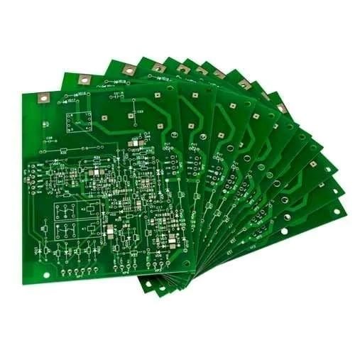
Types of Printed Circuit Boards
Printed Circuit Boards (PCBs) are an essential component in modern electronics. They provide a platform for connecting and supporting various electronic components, enabling the smooth flow of electrical signals. PCBs come in different types, each designed for specific applications and requirements. In this article, we will explore the various types of printed circuit boards and their uses.
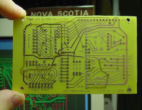
Single-Sided PCBs
Single-sided PCBs are the most basic and commonly used type of PCB. As the name suggests, they have copper traces on only one side of the board, while the other side is plain and without any components or traces. These boards are cost-effective and relatively simple to design and manufacture. Single-sided PCBs are commonly used in simple electronic devices with fewer components and lower circuit complexity, such as calculators, timers, and basic digital devices.
Double-Sided PCBs
Double-sided PCBs have copper traces on both sides of the board. This allows for a higher density of components and more complex circuit designs. The two sides of the board are connected through plated through-holes, which provide the necessary electrical connections between the layers. Double-sided PCBs are widely used in a variety of applications, including consumer electronics, telecommunications, and industrial equipment.
Multi-Layer PCBs
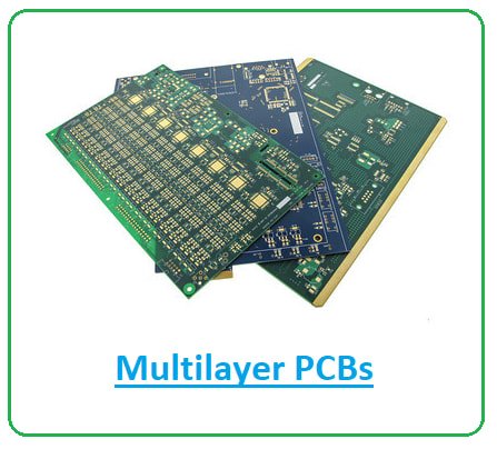
Multi-layer PCBs are the most complex and advanced type of PCB. They consist of multiple layers of copper traces separated by insulating material, typically referred to as the core and prepreg layers. The layers are bonded together using heat and pressure to create a single board with multiple interconnected layers. Multi-layer PCBs allow for even higher component density, increased circuit complexity, and improved signal integrity. They are commonly used in high-performance electronic devices, such as computers, smartphones, and medical equipment.
Rigid PCBs
Rigid PCBs are the most common type of PCB and are widely used in various applications. They are made of a solid, inflexible material, such as fiberglass-reinforced epoxy resin, which provides stability and durability to the board. Rigid PCBs are suitable for applications where the board needs to maintain its shape and structure, such as in most consumer electronics, automotive systems, and industrial equipment.
Flexible PCBs
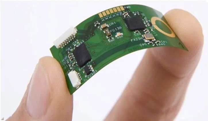
Flexible PCBs, also known as Flex PCBs or Flex Circuits, are designed to be highly flexible and bendable. They are made of thin, flexible materials, such as polyimide or polyester, that allow the board to conform to different shapes and contours. Flexible PCBs are ideal for applications where space is limited or where the board needs to be bent or folded, such as in wearable devices, medical implants, and aerospace systems.
Rigid-Flex PCBs
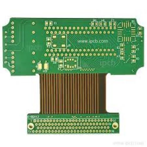
Rigid-Flex PCBs combine the benefits of both rigid and flexible PCBs. They consist of rigid sections interconnected by flexible sections, providing a versatile solution for complex circuit designs. Rigid-Flex PCBs are commonly used in applications that require a combination of rigid and flexible components, such as in smartphones, cameras, and military equipment.
The Process of Printed Circuit Board Design
Printed Circuit Board (PCB) design is a crucial step in the development of electronic devices. It involves creating a layout of interconnected electronic components on a board that allows for the smooth flow of electrical signals. The PCB design process requires careful planning, attention to detail, and adherence to industry standards. In this article, we will walk you through the steps involved in PCB design.
1. Requirements Gathering
The first step in PCB design is to gather the requirements for the circuit board. This involves understanding the functionality of the electronic device and the specific components that need to be integrated. It is important to have a clear understanding of the desired performance, size, and power requirements of the PCB.
During this phase, it is also important to consider any regulatory or compliance standards that the PCB must meet. This may include safety regulations, electromagnetic compatibility (EMC) standards, or environmental requirements.
2. Schematic Design
Once the requirements are gathered, the next step is to create a schematic diagram. The schematic diagram is a visual representation of the circuit that shows how the components are connected. It helps in understanding the functionality of the circuit and serves as a blueprint for the PCB layout.
During the schematic design phase, it is important to select the appropriate components and ensure that they are compatible with each other. It is also important to consider factors such as signal integrity, power distribution, and thermal management.
3. PCB Layout Design
After the schematic design is complete, the next step is to create the actual PCB layout. This involves placing the components on the board and routing the electrical connections between them.
During the PCB layout design phase, it is important to consider factors such as component placement, signal integrity, power distribution, and thermal management. The layout should be optimized to minimize signal interference, reduce power losses, and ensure efficient heat dissipation.
Modern PCB design software tools provide features such as auto-routing and design rule checking, which help in streamlining the layout design process and ensuring design accuracy.
4. Design Verification
Once the PCB layout is complete, it is important to verify the design for any errors or issues. This involves performing design rule checks, signal integrity analysis, and thermal analysis.
Design rule checks ensure that the layout adheres to the manufacturing capabilities of the PCB fabrication process. Signal integrity analysis helps in identifying potential issues such as noise, cross-talk, or signal distortion. Thermal analysis helps in identifying potential hotspots on the PCB and ensuring proper heat dissipation.
During the design verification phase, it is important to iterate and refine the design to address any issues that are identified. This may involve making changes to the component placement, routing, or power distribution.
5. PCB Fabrication
Once the design is verified and finalized, the next step is to send the design files to a PCB fabrication facility for manufacturing. The fabrication facility will use the design files to create the actual PCB.
During the PCB fabrication process, the design is transferred onto a copper-clad board, and the copper traces and pads are etched onto the board. This is followed by drilling holes for component mounting and applying a solder mask and silkscreen for component identification.
It is important to select a reputable PCB fabrication facility that can produce high-quality boards that meet the design specifications and industry standards.
6. PCB Assembly
Once the PCBs are fabricated, the next step is to assemble the electronic components onto the board. This involves soldering the components onto the PCB and ensuring proper alignment and connection.
PCB assembly can be done manually or using automated assembly equipment, depending on the complexity and volume of the production. It is important to follow industry standards and best practices to ensure reliable and efficient assembly.
7. Testing and Quality Assurance
After the PCB assembly is complete, the final step is to test the assembled boards for functionality and quality. This involves performing functional tests, electrical tests, and environmental tests to ensure that the PCB meets the desired performance and reliability requirements.
Testing and quality assurance are crucial to identify any defects or issues in the PCB and ensure that it performs as expected under different operating conditions.
How to Make a Printed Circuit Board?
Printed Circuit Boards (PCBs) are an essential component of modern electronics. They provide a sturdy and reliable platform for connecting various electronic components and allow for efficient electrical signal flow. Whether you are a hobbyist or a professional, learning how to make a PCB can be a valuable skill. In this blog post, we will guide you through the process of making a printed circuit board.
Gather Your Materials
Before you begin making a PCB, it’s important to gather all the necessary materials. Here’s a list of items you will need:
- Copper clad board
- Etching solution
- Acetone
- Transfer paper
- Iron
- Drill
- Drill bits
- Masking tape
- Sharpie or permanent marker
- Developer solution
- Etch resist pen
Create the PCB Design
The first step in making a PCB is to create a design. You can use various software tools such as Eagle, KiCad, or Altium Designer to design your PCB. These tools allow you to layout the components, define the traces, and generate the necessary files for fabrication.
Once you have your PCB design ready, you need to print it onto the transfer paper. Make sure to mirror the design so that it transfers correctly onto the copper clad board.
Transfer the Design
Now it’s time to transfer the design onto the copper clad board. Start by cleaning the board using acetone to remove any dirt or grease. Place the transfer paper with the design facing down onto the copper side of the board. Use masking tape to secure it in place.
Next, heat up the iron to a medium setting and press it firmly onto the transfer paper. Apply even pressure and move the iron around for about 5-10 minutes. This will transfer the design onto the copper clad board.
Etch the Board
After transferring the design, it’s time to etch the board. Etching is the process of removing the unwanted copper from the board, leaving only the traces and pads that make up your circuit.
Start by preparing the etching solution according to the manufacturer’s instructions. Wear protective gloves and goggles to ensure your safety. Place the copper clad board into the etching solution and agitate it gently. The etching process can take anywhere from a few minutes to half an hour, depending on the type and concentration of the etchant.
Once the unwanted copper has been etched away, remove the board from the etching solution and rinse it thoroughly with water. Use a scrub brush to remove any remaining etchant residue. Dry the board completely before proceeding to the next step.
Drill Holes
Now it’s time to drill holes for the components on your PCB. Use a drill with the appropriate drill bit size for your components. Start by marking the locations of the holes using a sharpie or permanent marker.
Secure the board in place and carefully drill the holes at the marked locations. Take your time and ensure that the holes are clean and free from any debris.
Apply Solder Mask
To protect the traces and pads on your PCB, it’s recommended to apply a solder mask. The solder mask prevents solder from flowing where it’s not intended to and provides an additional layer of insulation.
You can use an etch resist pen or a pre-made solder mask for this step. Apply the solder mask carefully and evenly over the entire board, making sure to cover all the traces and pads. Allow the solder mask to dry according to the manufacturer’s instructions.
Assemble and Test
With the solder mask applied, it’s time to assemble your PCB. Start by placing the components onto the board and soldering them in place. Take care to ensure that each component is properly aligned and soldered.
Once the components are soldered, it’s important to test your PCB for any potential issues. Use a multimeter to check for continuity, shorts, and proper voltage levels. Make any necessary adjustments or repairs before finalizing your PCB.
Conclusion
In conclusion, Making a printed circuit board can be a rewarding and fulfilling experience. By following the steps outlined in this blog post, you can create your own custom PCBs for your electronic projects. Remember to always prioritize safety and take your time to ensure a high-quality result. Happy PCB making.