Flexible Printed Circuit Boards
Introduction
Flexible printed circuit boards (PCBs) are a versatile and innovative solution for electronic devices that require a high level of flexibility and durability. These circuit boards are made from flexible materials, such as polyimide or polyester, which allow them to be bent, twisted, and folded without compromising their functionality. In this article, we will explore what flexible PCBs are, their advantages, applications, and why they are becoming increasingly popular in the electronics industry.
What are Flexible PCBs?
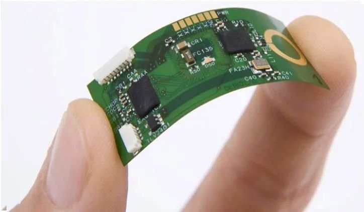
Flexible PCBs, also known as flex circuits or flexible printed circuit boards, are electronic interconnectivity solutions that offer flexibility in their design and usage. Unlike rigid PCBs, which are made from rigid materials like fiberglass or epoxy, flexible PCBs are made from flexible materials such as polyimide or polyester. These materials allow the PCBs to bend, twist, and conform to different shapes and contours, enabling them to fit into tight spaces or irregular shapes.
Types of Flexible PCBs
Flexible PCBs PCBs are made of a flexible plastic substrate, which allows them to be bent, twisted, and folded to fit into various shapes and sizes. Here are some different types of flexible PCBs and their uses in various industries:
1. Single-sided Flexible PCBs
Single-sided flexible PCBs are the simplest form of flexible PCBs. They consist of a single layer of conductive material, typically copper, on a flexible substrate. These PCBs are commonly used in applications where space is limited, and the circuit complexity is low. They are cost-effective and easy to manufacture, making them suitable for a wide range of applications, including consumer electronics, automotive, and medical devices.
2. Double-sided Flexible PCBs
Double-sided flexible PCBs have conductive material on both sides of the flexible substrate. This allows for more complex circuit designs and increased functionality. The two sides of the PCB are connected through vias, which are small holes drilled through the substrate. Double-sided flexible PCBs are widely used in applications that require higher circuit density and improved performance, such as smartphones, tablets, and wearable devices.
3. Multilayer Flexible PCBs
Multilayer flexible PCBs consist of three or more layers of conductive material separated by insulating layers. These PCBs offer the highest level of circuit density and functionality. The additional layers allow for the integration of more components and complex circuit designs. Multilayer flexible PCBs are commonly used in high-performance applications, such as aerospace, defense, and telecommunications.
4. Rigid-Flex PCBs
Rigid-flex PCBs combine the flexibility of flexible PCBs with the rigidity of traditional rigid PCBs. They consist of both flexible and rigid sections, which are interconnected through plated through-holes or flexible connectors. Rigid-flex PCBs offer the benefits of both types of PCBs, allowing for complex circuit designs that can be folded or bent to fit into tight spaces. They are commonly used in applications that require a combination of flexibility and durability, such as military equipment, industrial machinery, and medical devices.
5. Sculptured Flex PCBs
Sculptured flex PCBs are a specialized type of flexible PCBs that are designed to fit into unique or irregular shapes. They are created by selectively removing or etching the conductive material from the flexible substrate, leaving behind the desired circuit pattern. Sculptured flex PCBs are used in applications where standard flexible PCBs cannot meet the design requirements, such as curved displays, automotive interiors, and aerospace components.
What is Flexible PCB Coverlay?
Flexible PCB coverlay, also known as cover film or cover coat, is a protective layer that is applied onto the flexible circuit board. It acts as a barrier, protecting the circuitry from external elements such as moisture, dust, and chemicals. The coverlay is typically made of a polyimide material that provides flexibility and durability to the PCB.
The coverlay is applied to the flexible PCB using a lamination process. It is bonded to the circuitry and provides insulation and protection for the conductive traces and components. The coverlay is also responsible for defining the final shape and dimensions of the flexible PCB.
What is Solder Mask Layer?
The solder mask layer, also known as solder resist, is a thin protective coating that is applied over the copper traces on a PCB. Its primary purpose is to prevent solder from flowing onto areas where it is not intended during the soldering process. The solder mask layer is typically made of epoxy or a liquid photoimageable polymer.
The solder mask layer is applied to the PCB using a screen printing process or a liquid application method. It is then cured to form a protective coating that covers the exposed copper traces, leaving only the necessary areas for soldering exposed.
The Key Differences
Now that we understand the basic definitions of both the coverlay and the solder mask layer, let’s explore the key differences between the two:
Functionality: The coverlay provides insulation and protection for the flexible PCB, while the solder mask layer protects the copper traces from solder and other contaminants.
Material: The coverlay is typically made of a polyimide material, which provides flexibility and durability. On the other hand, the solder mask layer is made of epoxy or a liquid photoimageable polymer.
Application Process: The coverlay is applied to the flexible PCB using a lamination process, while the solder mask layer is applied using a screen printing process or a liquid application method.
Coverage: The coverlay covers the entire flexible PCB, providing insulation and protection to the entire circuitry. In contrast, the solder mask layer covers only the copper traces, leaving the necessary areas for soldering exposed.
Appearance: The coverlay is usually transparent or translucent, allowing visibility of the underlying circuitry. Conversely, the solder mask layer is typically green in color, although other colors such as red, blue, and black are also used.
A Step-by-Step Guide to Designing Flex PCBs
Designing flex PCBs requires careful planning, consideration of materials, and adherence to best practices. By following this step-by-step guide, you will be well-equipped to create successful flex PCB designs that meet your requirements and perform reliably. Remember to always consult with your PCB manufacturer and seek guidance from experienced designers to ensure the best possible outcome. Happy designing.
Step 1: Define Your Requirements
Before you start designing your flex PCB, it’s important to clearly define your requirements. Consider the following factors:
- Application: What is the intended use of the flex PCB? Understanding the application will help determine the necessary specifications, such as size, shape, and flexibility.
- Environment: Will the flex PCB be exposed to extreme temperatures, moisture, or other harsh conditions? This will impact the choice of materials and protective coatings.
- Electrical requirements: What are the voltage, current, and signal integrity requirements of your circuit? Ensure that your design meets these specifications.
- Manufacturing constraints: Consider the capabilities and limitations of your PCB manufacturer. This will help you design within their capabilities and avoid costly revisions.
Step 2: Choose the Right Materials
Choosing the right materials is crucial for the success of your flex PCB design. Here are some key considerations:
- Substrate material: The substrate material provides the base for the flexible circuit. Common options include polyimide (PI) and polyester (PET). Consider the mechanical, thermal, and electrical properties of each material.
- Copper thickness: The thickness of the copper layer affects the flexibility and conductivity of the flex PCB. Thicker copper is more rigid but offers better current-carrying capacity.
- Adhesive: The adhesive layer bonds the copper traces to the substrate. Choose an adhesive that provides good adhesion, flexibility, and thermal stability.
- Protective coatings: Depending on the application, you may need to apply protective coatings to enhance durability and resistance to moisture, chemicals, or temperature extremes.
Step 3: Design the Flex PCB
Now that you have defined your requirements and selected the materials, it’s time to design your flex PCB. Follow these steps:
- Schematic design: Create a schematic diagram of your circuit using a PCB design software. Ensure that all connections are correctly represented.
- Component placement: Place the components on the PCB layout, considering the space constraints and electrical requirements. Optimize the placement for signal integrity and thermal management.
- Routing: Route the traces between the components, taking care to avoid crossing or overlapping traces. Use curved traces instead of sharp angles to maintain flexibility.
- Ground and power planes: Include dedicated ground and power planes to ensure proper grounding and minimize noise interference.
- Test points: Add test points to facilitate testing and troubleshooting during the manufacturing and assembly process.
- Design rule check (DRC): Run a DRC to detect any design errors or violations, such as clearance violations or unconnected traces.
Step 4: Verify and Test
Once your design is complete, it’s important to verify and test the flex PCB before moving on to production. Consider the following steps:
- Design review: Have your design reviewed by a colleague or an experienced PCB designer to catch any potential errors or improvements.
- Prototype fabrication: Fabricate a prototype of your flex PCB to test its functionality and performance. Verify that it meets your electrical and mechanical requirements.
- Testing: Perform thorough testing, including electrical tests, environmental tests, and reliability tests, to ensure the quality and reliability of your flex PCB.
- Iterate and optimize: Based on the test results, make any necessary design iterations and optimizations to improve the performance and manufacturability of your flex PCB.
Advantages of Flexible PCBs
Flexible PCBs offer several advantages over traditional rigid PCBs, making them an attractive choice for many applications:
- Space Saving: Flexible PCBs are thin and lightweight, which makes them ideal for applications where space is limited. Their flexibility allows them to be folded or rolled, enabling efficient utilization of available space. This compactness is particularly beneficial in portable devices, wearable technology, and miniaturized electronics.
- Increased Reliability: Flexible PCBs have fewer interconnections and solder joints compared to rigid PCBs, reducing the risk of failure due to loose connections or broken solder joints. The absence of connectors and cables also minimizes the chances of signal loss or electromagnetic interference, resulting in improved reliability and performance.
- Enhanced Durability: The flexible materials used in PCB manufacturing provide excellent resistance to vibrations, shocks, and extreme temperatures. This durability makes flexible PCBs suitable for applications that require high reliability and performance in harsh environments.
- Design Flexibility: Flexible PCBs offer designers the freedom to create complex and intricate circuitry layouts that are not possible with rigid PCBs. The ability to bend and flex the PCBs allows for three-dimensional designs, enabling efficient use of available space and simplified assembly processes.
- Cost Savings: Although the initial manufacturing cost of flexible PCBs may be higher than rigid PCBs, the overall cost can be lower in certain applications. The elimination of connectors, cables, and additional components reduces assembly time and materials, resulting in cost savings in the long run.
Applications of Flexible PCBs
The unique characteristics of flexible PCBs make them suitable for a wide range of applications across various industries. Some common applications include:
- Consumer Electronics: Flexible PCBs are widely used in smartphones, tablets, laptops, and wearable devices due to their compact size and lightweight nature. They enable the seamless integration of electronic components in these devices while providing the necessary flexibility for user comfort.
- Automotive Industry: In the automotive industry, flexible PCBs are used in applications such as dashboard displays, lighting systems, engine control units, and sensors. Their ability to withstand vibrations and extreme temperatures makes them ideal for automotive environments.
- Medical Devices: Flexible PCBs are extensively utilized in medical devices such as pacemakers, diagnostic equipment, and wearable health monitors. Their flexibility allows for comfortable integration into the human body, while their reliability ensures accurate and consistent performance.
- Aerospace and Defense: Flexible PCBs are used in aerospace and defense applications where lightweight and reliable interconnectivity solutions are required. They are used in satellites, aircraft systems, military equipment, and communication devices.
- Industrial Automation: In industrial automation, flexible PCBs are used in control systems, robotics, sensors, and monitoring equipment. Their durability and flexibility make them suitable for demanding industrial environments.
Conclusion
In conclusion, Flexible PCBs have revolutionized the electronics industry by offering a flexible and versatile alternative to traditional rigid PCBs. Their space-saving design, increased reliability, enhanced durability, design flexibility, and cost savings make them an excellent choice for a wide range of applications. As technology continues to advance, the demand for flexible PCBs is expected to grow, driving further innovation in this field.