How to Reduce Ripple of Switching Power Supply?
Understanding ripple is crucial in power supply design because excessive ripple can lead to various issues in electronic circuits. High levels of ripple can introduce noise, causing interference and degrading signal integrity. Furthermore, sensitive components may suffer from performance degradation or even damage due to the fluctuating voltage levels. Therefore, controlling ripple is essential to ensure the stable and reliable operation of electronic devices. In this blog post, we will learn how to reduce ripple of switching power supply!
What is Ripple in Switching Power Supplies?
Ripple in switching power supplies refers to the residual periodic variation, or AC component, found in the DC output voltage. This phenomenon is an inherent aspect of the power conversion process, resulting from the switching action of the power supply. Ripple is typically characterized by its frequency and amplitude, both of which can impact the performance and reliability of electronic circuits.
The primary sources of ripple include the switching action of the power supply and the characteristics of its components, such as inductors, capacitors, and transformers. During the switching process, rapid transitions between on and off states create oscillations that manifest as ripple in the output voltage. The effectiveness of the components in filtering these oscillations largely determines the magnitude of the ripple.
Types of Ripple
There are two main types of ripple to consider: low-frequency ripple and high-frequency ripple. Low-frequency ripple is generally associated with the input power frequency, often originating from the rectification of AC mains voltage. This type of ripple has a frequency typically around 50 or 60 Hz, depending on the local power grid. On the other hand, high-frequency ripple is related to the switching frequency of the power supply, which can range from tens of kilohertz to several megahertz. High-frequency ripple is a direct result of the rapid switching cycles and is usually more challenging to filter effectively.
Methods for Measuring and Reducing Ripple
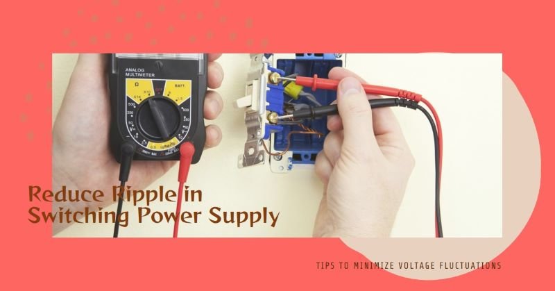
Accurately measuring ripple in switching power supplies is pivotal for ensuring optimal performance and reliability. The primary tools used for this purpose include oscilloscopes and spectrum analyzers. Oscilloscopes are instrumental in visualizing the time-domain characteristics of ripple, allowing engineers to observe amplitude fluctuations and transient responses. Spectrum analyzers, on the other hand, offer insight into the frequency-domain properties, enabling the identification of specific harmonic content associated with ripple. These instruments together provide a comprehensive understanding of both amplitude and frequency characteristics of ripple, crucial for effective mitigation strategies.
To reduce ripple, various design and component selection strategies are employed. One fundamental approach is the use of low Equivalent Series Resistance (ESR) capacitors. These capacitors minimize resistive losses, thereby reducing ripple voltage. Inductors are also critical; they store energy and smooth out current fluctuations, contributing to lower ripple. Additionally, snubber circuits, which typically consist of a resistor-capacitor (RC) network, help in damping high-frequency oscillations, further mitigating ripple.
Advanced techniques such as synchronous rectification and active filtering are also effective. Synchronous rectification replaces traditional diodes with controlled switches, significantly improving efficiency and reducing ripple. Active filtering, involving feedback control systems, dynamically adjusts the filtering parameters to maintain minimal ripple under varying load conditions.
Capacitor Ripple and Inductor Ripple
Capacitor ripple arises from the charging and discharging cycles of capacitors during switching operations. When a capacitor charges, it stores energy, and upon discharging, it releases this energy, creating a fluctuating voltage. The magnitude of this ripple is significantly influenced by the capacitor’s Equivalent Series Resistance (ESR). A higher ESR results in greater voltage fluctuations, thereby increasing the ripple. These fluctuations can be visually represented by waveforms, where the peaks and troughs illustrate the capacitor’s charging and discharging cycles.
On the other hand, inductor ripple is generated through the continuous energy storage and release during each switching cycle. Unlike capacitors that charge and discharge, inductors store energy in their magnetic field when current flows through them. As the current alternates, the inductor releases this stored energy, leading to a ripple in the current and, consequently, the output voltage. The waveform of inductor ripple typically shows a more continuous and smoother oscillation compared to capacitor ripple.
Switching Noise and Load Transients
Switching noise, a common phenomenon in switching power supplies, arises from the rapid on/off transitions of switches. This high-frequency noise can interfere with the proper functioning of electronic circuits, leading to potential issues in overall system performance. The primary sources of switching noise include parasitic inductance and capacitance inherent in the circuit layout. These parasitics can generate unintended oscillations and electromagnetic interference (EMI), which can propagate through the power supply and affect other components.
To minimize switching noise, several techniques are employed. One effective method is the use of snubber circuits, which are designed to dampen oscillations and absorb excess energy. Proper PCB layout practices, such as minimizing loop areas and ensuring tight coupling of return paths, can significantly reduce the impact of parasitic elements. Additionally, shielding sensitive components and critical signal paths can help mitigate the effects of EMI, thereby enhancing the overall stability of the power supply.
Load transients, on the other hand, refer to sudden changes in the load demand that can cause voltage fluctuations in the power supply output. These fluctuations occur because the power supply needs time to adjust to the new load conditions, which can result in temporary instability. The dynamics of load transients are influenced by factors such as the load step size, the response time of the power supply, and the characteristics of the feedback control mechanisms in place.
Filtering Techniques for Ripple Reduction
Various filters, including low-pass filters, LC filters and RC filters, offer distinct advantages in achieving this goal.
Low-pass filters are among the simplest and most commonly used methods for ripple reduction. These filters allow low-frequency signals to pass through while attenuating high-frequency components. They are highly effective in smoothing out the output voltage, especially in applications where the ripple frequency is significantly higher than the signal frequency. The primary design considerations for low-pass filters include selecting the appropriate cutoff frequency and ensuring that the chosen components can handle the expected current and voltage levels. Capacitors and inductors are critical in this design, with their values determining the filter’s effectiveness.
LC filters, which combine inductors (L) and capacitors (C), offer superior ripple attenuation compared to low-pass filters alone. The inductor blocks high-frequency ripple, while the capacitor provides a low-impedance path to ground for these frequencies. This dual action significantly reduces ripple amplitude. However, the design of LC filters requires careful consideration of the inductor’s series resistance and the capacitor’s equivalent series resistance (ESR), as these factors can impact overall efficiency. Additionally, the physical placement of these components on the PCB can affect performance, with proximity to noise sources potentially degrading filter efficacy.
RC filters, consisting of resistors (R) and capacitors (C), are another effective method for ripple reduction. These filters are particularly useful in applications where size and cost constraints are critical. The resistor in the RC filter provides a damping effect, while the capacitor shunts high-frequency noise to ground. When designing RC filters, the resistor value must be chosen to balance between adequate ripple reduction and acceptable power dissipation. Similarly, the capacitor value should be selected based on the desired cutoff frequency and the application’s voltage requirements.
Practical applications and case studies highlight the effectiveness of these filtering techniques. For instance, in a DC-DC converter for a communication device, implementing an LC filter reduced the output ripple by over 90%, ensuring stable operation of sensitive components. Similarly, in a power supply for medical equipment, a combination of low-pass and RC filters achieved the necessary ripple specifications, enhancing overall device reliability.
Optimizing PCB Layout to Minimize Ripple
Optimizing the printed circuit board (PCB) layout is a crucial step in reducing ripple in switching power supplies. An effective PCB layout can significantly minimize electromagnetic interference (EMI) and enhance overall performance. Here, we delve into key principles of good PCB design that help achieve these goals.
Firstly, minimizing loop areas is essential. Large loop areas can act as antennas, picking up and radiating EMI. To mitigate this, keep the power and ground loops as small as possible. This involves placing high-frequency components, such as decoupling capacitors, close to the power pins of integrated circuits to reduce the loop area.
Proper grounding techniques are another critical aspect. Implementing a solid ground plane can provide a low-impedance path for return currents, significantly reducing noise and ripple. Additionally, it is beneficial to use multiple ground vias to ensure a robust connection between different layers of the PCB. Avoid creating ground loops and ensure that all ground points are connected to a single reference point.
The strategic placement of components can also influence ripple reduction. High-frequency components should be placed as close to each other as possible to minimize the length of high-current paths, thereby reducing inductive and capacitive couplings. For instance, placing the switching transistor, inductor, and output capacitor in close proximity can help in achieving a compact layout that minimizes ripple.
To avoid common layout mistakes, ensure that the power traces are wide enough to handle the current without significant voltage drops. Moreover, avoid routing sensitive signal traces near high-frequency switching nodes to prevent coupling and interference. Incorporating these layout strategies can lead to significant reductions in ripple and EMI, enhancing the performance and reliability of switching power supplies.
Advanced Control Strategies for Ripple Mitigation
Advanced control strategies, such as feedback control loops and pulse-width modulation (PWM), play a significant role in achieving this goal. Implementing these techniques effectively reduces output voltage fluctuations and enhances the overall stability of the power supply.
Feedback control loops are among the most widely used methods for ripple mitigation. These loops continuously monitor the output voltage and compare it to a reference value. When deviations are detected, the control loop adjusts the duty cycle of the switching transistor to correct the output. This real-time adjustment helps maintain a stable output voltage, thereby reducing ripple. A well-designed feedback control loop can significantly enhance the performance of a switching power supply by minimizing transient responses and ensuring rapid return to steady-state conditions.
Pulse-width modulation (PWM) is another critical technique in ripple mitigation. PWM controls the average voltage delivered to the load by varying the width of the pulses in the power signal. By adjusting the duty cycle, PWM can effectively regulate the output voltage and minimize ripple. This technique is highly efficient and widely adopted in modern power supply designs due to its simplicity and effectiveness.
In addition to feedback control loops and PWM, other advanced techniques such as current-mode control and digital control methods also contribute to ripple reduction. Current-mode control monitors the inductor current and adjusts the duty cycle accordingly, providing faster response to load changes and further reducing ripple. Digital control methods leverage microcontrollers or digital signal processors (DSPs) to implement complex control algorithms that can adapt to varying operating conditions, enhancing the power supply’s performance and stability.
Real-world examples and case studies highlight the effectiveness of these advanced control strategies. For instance, a telecommunications equipment manufacturer implemented a combination of PWM and current-mode control in their power supply design, resulting in a 50% reduction in output ripple. Similarly, a consumer electronics company utilized digital control methods to achieve precise voltage regulation and improved overall system reliability.
Conclusion
In summary, controlling ripple in switching power supplies is essential for keeping electronic circuits stable and reliable. Too much ripple can cause noise, interfere with signals, and damage sensitive parts. By understanding what causes ripple and using tools to measure it, engineers can find ways to reduce it.
Effective methods include using low ESR capacitors, inductors, and snubber circuits, along with advanced techniques like synchronous rectification and active filtering. Good PCB layout and control strategies like feedback loops and pulse-width modulation also help minimize ripple. By applying these techniques, engineers can significantly reduce ripple, ensuring electronic devices work efficiently and reliably.
