A Complete Guide to IC Package Technology
Over the years, IC packaging technology has undergone significant advancements. From the early days of simple dual in-line packages (DIPs) to the sophisticated and compact ball grid arrays (BGAs) and chip-scale packages (CSPs) of today, the evolution has been driven by the need for higher performance, miniaturization and better thermal management. These advancements reflect the continuous effort to meet the growing demands of the electronics industry, enabling the development of more powerful, efficient and compact electronic devices. This guide will help you understand the different types of IC packages, their sizes, and key technologies like Surface Mount Device (SMD), Ball Grid Array (BGA), and Through Hole Technology (THT)
What is IC Package?
An IC package is essentially the housing of an integrated circuit chip. It provides the physical means for the chip to be connected to a printed circuit board (PCB). The packaging not only protects the chip but also aids in heat dissipation and electromagnetic shielding. Depending on the application, IC packages can vary significantly in size, shape and material.
IC packages provide a structured interface through which the internal circuitry of the semiconductor can communicate with the external environment. This is accomplished by incorporating leads or pins that connect to the printed circuit board (PCB), facilitating the seamless transmission of electrical signals. The design and arrangement of these connections are critical, as they influence the efficiency and speed of the data transfer, directly impacting the functionality of the end product.
Types and Sizes of IC Packages
IC packages come in various types and sizes, each tailored for specific applications and performance requirements. Here are some common types:
Surface Mount Device (SMD)
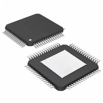
Surface mount devices are designed for mounting directly onto the surface of printed circuit boards (PCBs). They are highly favored in modern electronics due to their compact size, which allows for higher circuit density and improved performance.
- QFP (Quad Flat Package):
- Larger PCB footprint, commonly used for ICs and integrated circuits.
- Sizes include 7x7mm, 10x10mm, 14x14mm, etc.
- Pin count ranges from dozens to hundreds.
- BGA (Ball Grid Array):
- Spherical pads with package pitch ranging from 0.75mm to 1.0mm.
- Pin count varies from dozens to hundreds.
- Suitable for high-performance chips and large-scale integrated circuits, offering excellent heat dissipation and electrical performance.
- SOIC (Small Outline Integrated Circuit):
- Compact shape and small pitch pin layout, ideal for medium-sized integrated circuits.
- Sizes typically are 3x3mm, 5x5mm, 7x7mm.
- Pin count generally ranges from 8 to 48.
Plug-in Packaging (THT) – Through Hole Technology
Through-hole technology involves inserting component leads through holes in the PCB and soldering them in place. Although THT components are generally larger than SMDs, they offer excellent mechanical strength, making them suitable for applications subjected to mechanical stress.
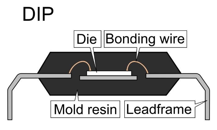
- DIP (Dual Inline Package):
- Common size is 7.62mm (0.3 inches) pitch.
- Pin count ranges from 8 to hundreds.
- TO-220 Packages:
- Typically used for power devices.
- Approximately 10x15mm in size with three pins.
- TO-92:
- Dimensions are approximately 5x5mm.
- Usually has a pin count of 3.
Other Package Types
- COB (Chip on Board):
- Chip directly mounted on the PCB.
- Package size is very small, suitable for compact equipment and products with high integration requirements.
- PLCC (Plastic Leaded Chip Carrier):
- Used for highly integrated digital circuits.
- Package size is approximately 20x20mm.
- Pin count usually ranges from 20 to 84.
Essential Information in IC Packaging
IC packaging contains crucial information necessary for the design and production of PCB boards. This includes:
Package Type: Indicates the package type such as QFP, BGA, SMD, etc.
Package Size: Describes overall dimensions (length, width, height).
Pin Layout: Arrangement of pins (single row, double row, grid, etc.).
Pin Count: Number of pins, influencing the component’s functionality and interfaces.
Material Type: Packaging materials (plastic, ceramic) affecting mechanical strength and heat resistance.
Pad Information: Location, shape, and size of solder pins.
Thermal Management: Parameters for heat dissipation structures.
Package Identification: Manufacturer’s logo, model number, date code.
Pin Function: Description of pin functions for complex packages.
Environmental Adaptability: Characteristics like waterproofing and dustproofing.
This information ensures proper integration of components into the circuit, meeting design requirements and performance specifications.
International Standards for IC Packaging
Certain internationally applicable standards define packages, schematic symbols, and 3D models:
- IPC 7351 (PCB Packaging): Defines physical size, pin layout, and pad design of standard SMD component packages.
- ANSI Y32.2-1975 (Schematic Symbols): Defines symbols for various electrical components, aiding in schematic design.
- ISO 10303-21 (3D Model): Specifies the file format for STEP models, facilitating 3D CAD software integration.
Rules to Follow When Designing IC Packages
Package Size: Ensure size and shape match component specifications.
Pin Arrangement: Avoid overlapping and ensure sufficient spacing for soldering.
Pad Design: Correct pad size and shape for welding quality and reliability.
Thermal Management: Design appropriate heat dissipation structures.
Symbol Marking: Accurate symbolic representation in schematics.
3D Model: Provides a 3D representation for PCB layout and collision detection.
Prohibited Areas: Designate sufficient areas to prevent collisions.
Manufacturability Considerations: Align design with manufacturing and assembly processes.
How to Choose the Correct IC Package
1. Different IC Packaging Types
- Surface Mount Technology (SMT): Suitable for small electronic products like smartphones and tablets.
- Plug-in Packaging: Ideal for larger electrical and mechanical connections in industrial control systems and automotive electronics.
- System-in-Package (SiP): Integrates multiple functional modules for higher integration and performance.
- Ball Grid Array (BGA): High-density solder ball array for high-performance and high-power applications.
2. Determine Functional and Performance Requirements
- Signal Integrity: Ensure package meets signal quality and stability requirements, especially for high-frequency or high-speed signals.
- Size Restrictions: Match package size to PCB layout to prevent installation issues.
3. Consider Cooling and Thermal Management
- Heat Dissipation: Choose packages with effective heat dissipation designs to prevent overheating.
4. Consider Layout and Routing
- Pin Layout: Ensure package matches PCB layout for good signal integrity and electrical connections.
5. Cost and Supply Chain Availability
- Cost vs. Performance: Balance cost with performance and ensure availability to meet project requirements and timelines.
Conclusion
In conclusion, IC packaging plays an imp role in the performance, reliability, and integration of electronic components. Understanding the different types of packages, their sizes, and the standards governing them is essential for designing effective and efficient electronic systems.