11 Types of Printed Circuit Board Raw Material Specification
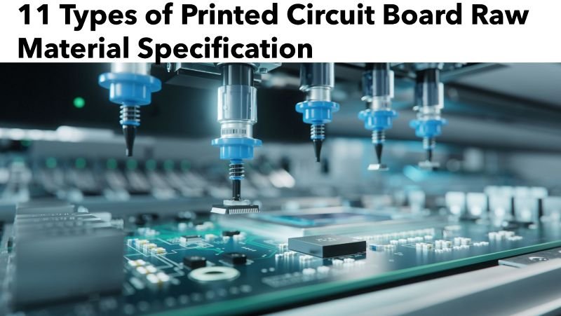
Printed Circuit Boards (PCBs) are the backbone of modern electronic devices, providing the physical and electrical connections for components to work together. The performance, reliability and longevity of PCBs are significantly influenced by the raw materials used in their manufacture. Understanding the specifications and characteristics of these materials is essential for designing high-quality PCBs that meet the required functional standards. In this article, we’ll discuss essential raw materials used in PCB manufacturing:
1. Copper Clad Laminates (CCL)
Description and Function: Copper Clad Laminates (CCLs) are essential in the construction of PCBs, acting as the base layer for the copper circuitry. These laminates are made of a dielectric substrate material (such as fiberglass) that is bonded to a thin layer of copper foil. The copper layer serves as the conductive path for electrical signals, and CCLs play a crucial role in determining the electrical and mechanical properties of the finished PCB. The CCL is then etched to create the traces that interconnect electronic components.
Specifications:
- Thickness: The thickness of CCLs can vary depending on the type of PCB design. Common thicknesses range from 0.2 mm to 2 mm. The thickness impacts the mechanical stability and flexibility of the PCB.
- Copper Weight: This refers to the weight of copper per unit area, typically measured in ounces per square foot (oz/ft²). Common copper weights include 1 oz/ft², 2 oz/ft², and 3 oz/ft². Higher copper weight allows for better current-carrying capacity but can affect the flexibility of the board.
- Surface Finish: The surface finish of CCL is crucial for soldering and component attachment. Different finishes, such as matte, smooth, and rough, influence the ease of soldering, conductivity, and durability of the PCB. The surface roughness impacts how well solder adheres to the copper layer, with rougher surfaces promoting better solder joints.
Types of Copper-Clad Laminates Used in PCBs:
- Standard CCL: Made with a fiberglass substrate and copper foil, suitable for most standard PCB applications.
- High-Frequency CCL: Designed for applications requiring stable electrical properties at high frequencies, such as in RF circuits.
- Heavy Copper CCL: These are used for power PCBs, which require thicker copper for higher current applications.
- Halogen-Free CCL: Made without halogens to comply with environmental standards like RoHS.
2. Base Material (Substrate)
Description of Different Types (FR4, CEM1, etc.): The base material, or substrate, forms the core structure of the PCB and provides the support for copper traces and components. The most commonly used substrates include:
- FR4: This is the most widely used PCB substrate, made of woven fiberglass cloth impregnated with epoxy resin. It offers a good balance of electrical performance, mechanical strength, and cost-effectiveness.
- CEM1 (Composite Epoxy Material): CEM1 is a cheaper alternative to FR4, made of paper-based material and epoxy resin. It is commonly used in low-cost, single-layer PCBs.
- CEM3: A newer material, similar to FR4 but with better thermal stability and resistance to high temperatures. It is used in medium- to high-end applications.
- Polyimide: Used for flexible PCBs, polyimide substrates offer flexibility and higher thermal stability than FR4.
- PTFE (Teflon): Known for its low dielectric constant and excellent performance at high frequencies, PTFE is used in high-frequency applications like RF PCBs.
Key Specifications:
- Dielectric Constant: The dielectric constant (Dk) measures the material’s ability to transmit electrical signals. Low Dk materials are preferred for high-frequency applications, as they reduce signal loss and delay.
- Flame Resistance: A critical property for ensuring that PCBs meet safety standards. The flame-retardant grade (such as UL94V-0) indicates the material’s ability to resist combustion.
- Thermal Stability: The substrate material’s ability to withstand high temperatures without degrading is crucial for reliability in power and high-performance applications.
How Substrate Material Affects PCB Performance: The choice of substrate impacts the thermal conductivity, mechanical strength, and electrical properties of the PCB. For instance, FR4 is durable and versatile but may not perform well at very high frequencies or in extremely hot environments. In contrast, PTFE substrates are ideal for high-frequency applications but come at a higher cost. The substrate’s dielectric constant affects the signal integrity, especially for high-speed digital circuits.
3. Resins
Types of Resins (Epoxy, Phenolic, etc.): Resins are used in PCBs to bind the materials together and provide structural integrity. The type of resin selected can affect the board’s strength, thermal resistance, and overall performance. Some common types of resins used in PCB manufacturing include:
- Epoxy Resin: The most common resin used in PCB manufacturing. It provides good mechanical strength, thermal resistance, and electrical insulation properties.
- Phenolic Resin: Typically used in low-cost PCBs. It is less durable than epoxy but is inexpensive and suitable for simple, low-performance applications.
- Polyimide Resin: Used in flexible PCBs, offering high thermal stability and flexibility.
- Acrylic Resin: Known for its transparency and UV stability, it is used for specialized applications like LED PCBs.
Role in PCB Manufacturing: Resins are primarily used to bond the various layers of the PCB, ensuring the integrity of the board during manufacturing and throughout its operational life. They also play a role in providing insulation between the copper layers and preventing short circuits. The resin material helps define the thermal stability and mechanical strength of the PCB.
Specifications:
- Temperature Resistance: The resin should withstand the temperature of the PCB’s operating environment without degrading. Epoxy resins, for instance, typically withstand temperatures up to 130°C, while polyimide resins can handle temperatures above 200°C.
- Mechanical Strength: The resin should provide adequate mechanical strength to withstand physical stresses without cracking or deforming.
- Curing Temperature: Resins need to be cured at specific temperatures to achieve the required properties. For epoxy resins, this is typically between 120°C and 180°C, depending on the type.
4. Solder Mask
Function of Solder Mask in PCB: Solder mask is a protective layer applied to the PCB to prevent solder from bridging between copper traces and to protect the board from environmental factors like moisture and dirt. It also aids in the mechanical protection of the board and enhances its electrical insulation properties. The solder mask helps define the areas where components will be soldered by preventing solder from sticking to unwanted areas.
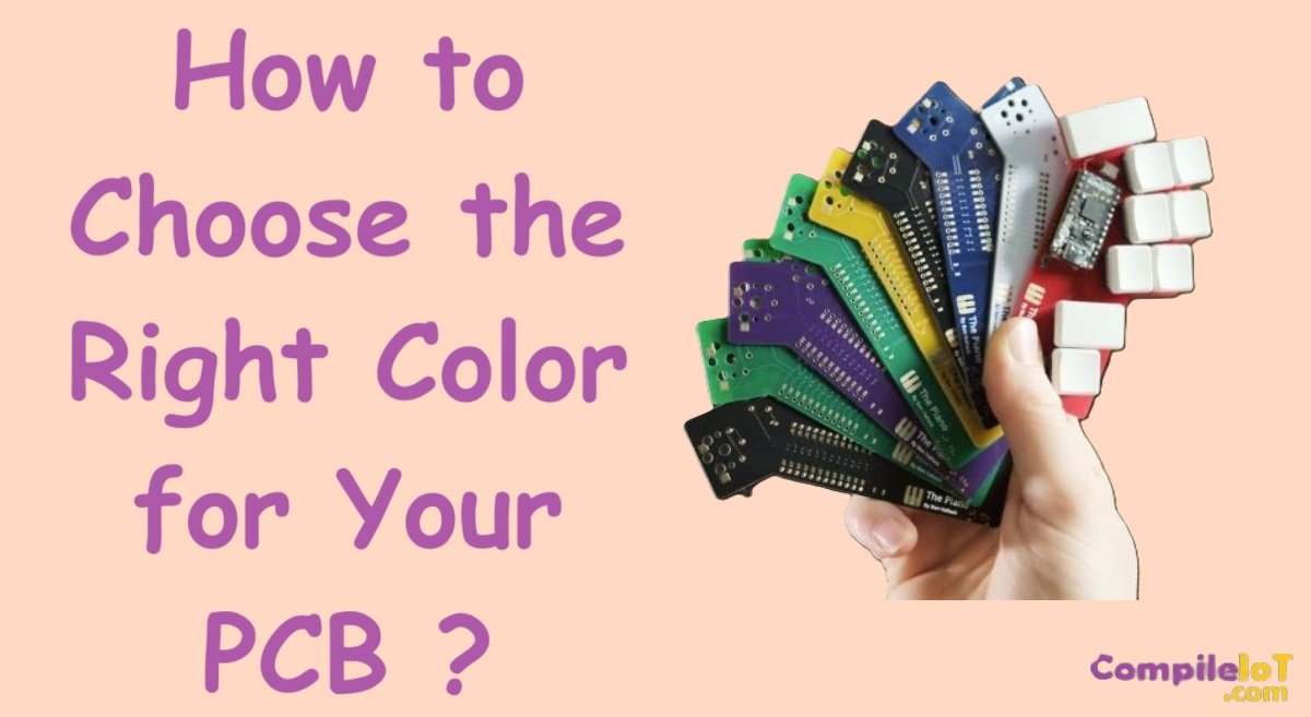
Types (Green, Black, Blue, etc.):
- Green Solder Mask: The most common color used in PCB manufacturing. It is durable, easily visible, and cost-effective.
- Black Solder Mask: Often used for aesthetic purposes or in designs where high contrast is needed for easier inspection.
- Blue and Red Solder Masks: These are sometimes used for specialized applications or for visual distinction.
- White Solder Mask: Used in some applications, but less common due to its susceptibility to dirt.
Specifications:
- Thickness: The typical thickness of solder mask layers ranges from 15 to 35 microns, depending on the board’s requirements. Thicker layers provide better protection, but too thick a layer can cause issues with fine-pitch components.
- Curing Temperature: Solder mask must be cured to ensure it adheres properly to the PCB. The curing temperature typically ranges from 130°C to 150°C, depending on the material.
- Surface Finish: The finish of the solder mask affects the ease of soldering and the reliability of solder joints. A smooth, consistent finish is ideal for good solder flow and reliable connections.
5. Silkscreen
Role of Silkscreen in PCB Design: Silkscreen is an ink layer applied to the surface of a PCB to add labels, component outlines, and other textual markings. It serves several essential purposes in PCB design:
- Identification: Component names, values, and other markings help technicians and engineers identify components and troubleshoot the board.
- Aesthetic and Documentation: It provides a clean, professional appearance and is often used for branding or providing additional information, such as logos or part numbers.
- Assembly Guidance: The silkscreen layer aids during assembly by indicating the location of components and helping prevent mistakes.
Materials Used (Ink Types):
- Epoxy-based Inks: These are commonly used for their excellent adhesion properties and durability. They are resistant to high temperatures and chemical exposure, making them ideal for long-lasting marks on PCBs.
- UV-Curable Inks: These inks cure quickly under ultraviolet light, making them ideal for high-speed manufacturing processes. They offer good adhesion and resistance to environmental factors.
- Lead-Free Inks: These inks are compliant with RoHS (Restriction of Hazardous Substances) and are used in environmentally conscious manufacturing processes.
Specifications (Ink Consistency, Visibility, Resistance):
- Ink Consistency: The consistency of the ink is essential to ensure a smooth, even application on the PCB. It should be thick enough to stay in place but not too thick to cause smudging or poor resolution of text.
- Visibility: The ink must have high contrast against the background of the PCB to ensure that markings are clearly visible for assembly and inspection. Common colors include white, yellow, and black.
- Resistance: Silkscreen ink must be resistant to heat, chemicals, and wear. The ink should be able to withstand the soldering process and exposure to environmental conditions without fading or peeling off.
6. Copper Foil
Role and Importance in PCB Design: Copper foil is a critical component of PCBs, providing the conductive pathways that carry electrical signals between components. It is bonded to the PCB substrate (typically via copper-clad laminates) and etched to create the circuit design. Copper foil plays a vital role in the electrical performance, thermal dissipation, and overall functionality of the PCB. Its quality and thickness directly affect the current carrying capacity and signal integrity of the PCB.
Types (Electrolytic, Rolled):
- Electrolytic Copper Foil: This type of foil is produced through an electroplating process, where copper ions are deposited onto a substrate. It generally has a rougher surface, which is suitable for high-adhesion applications in PCBs with thicker copper layers.
- Rolled Copper Foil: Rolled foil is created by mechanically rolling copper to thin sheets. It is often smoother than electrolytic copper foil and is used in PCBs requiring fine trace patterns or when a more uniform surface is needed for better soldering quality.
Specifications (Thickness, Surface Roughness):
- Thickness: Copper foil thickness is typically measured in ounces per square foot (oz/ft²), which indicates the weight of copper foil used. Common thicknesses include 1 oz/ft² (about 35 microns) for standard PCBs, with heavier weights (2 oz/ft², 3 oz/ft², etc.) used for high-power PCBs that carry higher current.
- Surface Roughness: The surface roughness of copper foil influences how well it adheres to the substrate and how effectively solder bonds to it. Electrolytic copper generally has a rougher surface than rolled copper, which can be advantageous for certain types of PCB designs but may be less suited for high-frequency applications where smooth surfaces are preferred to minimize signal loss.
7. Via Materials
Overview of Vias in PCB Design: Vias are small holes drilled through a PCB that allow electrical signals to pass between different layers of the board. They are essential for multi-layer PCBs, where different electrical paths are needed on separate layers of copper. Vias help connect components on different layers, providing interconnects for power, ground, and signal traces.
Types of Via Materials Used (Copper, Silver):
- Copper: Copper is the most common material used in vias due to its excellent electrical conductivity and cost-effectiveness. It is used to fill the vias after they are drilled, ensuring low resistance and high current-carrying capacity.
- Silver: Silver-filled vias are used in high-performance applications where ultra-low resistance and high conductivity are essential. They are often used in high-frequency or high-speed PCBs, such as RF applications, to minimize signal degradation.
Specifications (Electrical Conductivity, Durability):
- Electrical Conductivity: Copper is the standard material used for vias due to its high electrical conductivity, which ensures efficient signal and power transmission. Silver vias, while more expensive, offer even higher conductivity and are used in applications requiring minimal resistance.
- Durability: Vias must be durable enough to withstand the thermal stresses of soldering and the mechanical stresses during assembly and operation. The material used for vias should be resistant to corrosion and fatigue, ensuring long-lasting electrical connections.
8. Conductive Adhesives
Role of Conductive Adhesives in PCB Assembly: Conductive adhesives are used to attach electronic components to the PCB, particularly in places where traditional soldering is difficult or not ideal. These adhesives provide a conductive path between the component leads and the PCB, enabling electrical connections without requiring heat or a soldering process. Conductive adhesives are used in sensitive components, flexible PCBs, or areas that may not tolerate the high temperatures of soldering.
Specifications (Conductivity, Curing Temperature, Viscosity):
- Conductivity: The adhesive must have high conductivity to ensure that the electrical signal passes reliably between the component and the PCB. The conductivity is typically measured in ohm-centimeters (Ω·cm) and should be low enough to provide a reliable electrical path.
- Curing Temperature: Conductive adhesives need to be cured at specific temperatures to ensure the proper formation of conductive bonds. The curing temperature typically ranges from 120°C to 180°C, depending on the adhesive formulation.
- Viscosity: The viscosity of the adhesive is essential to ensure proper application without excess spilling. A lower viscosity allows the adhesive to flow smoothly into the connection areas, while a higher viscosity ensures that the adhesive stays in place during assembly.
Types and Applications:
- Epoxy-based Conductive Adhesives: These are widely used for their strong bonding capabilities and ability to withstand mechanical and thermal stresses. They are commonly used for attaching components in flexible and rigid-flex PCBs.
- Silver-filled Adhesives: These adhesives provide excellent conductivity and are often used in high-performance applications like RF circuits or in conditions requiring minimal resistance.
- Pressure-sensitive Adhesives: These are used for quick and easy component placement, where heat or curing processes may not be feasible.
9. Plating Materials
Types of Plating Materials Used in PCBs (Gold, Silver, Tin, etc.): Plating materials are used to coat the PCB’s copper surfaces to improve their performance in terms of durability, electrical conductivity, and corrosion resistance. Common plating materials include:
- Gold: Often used for its excellent conductivity and corrosion resistance, gold plating is applied in high-performance applications like connectors, ICs, and other components where durability and reliability are critical.
- Silver: Silver plating offers the highest electrical conductivity among all metals and is used in RF, high-frequency, and high-speed PCB designs.
- Tin: Tin plating is used for surface finishes like HASL (Hot Air Solder Leveling) to provide a protective layer against oxidation and to facilitate soldering.
- Nickel: Nickel is often used as an underlayer beneath gold plating (as in ENIG – Electroless Nickel Immersion Gold) to provide added strength and resistance to wear.
Specifications (Thickness, Conductivity):
- Thickness: The thickness of the plating layer depends on the application. For instance, gold plating for connectors may range from 0.2 to 5 microns, while tin plating may vary from 20 to 100 microns. The plating thickness affects the durability and the quality of the electrical connection.
- Conductivity: The primary goal of plating materials is to improve the electrical conductivity of the PCB. Gold and silver provide the best conductivity, making them ideal for high-performance and high-frequency applications. Nickel offers a balance between conductivity and mechanical strength, while tin is used for its ease of soldering.
Importance in Improving Reliability and Performance: Plating materials not only enhance the electrical performance of the PCB but also improve its longevity and resistance to corrosion, oxidation, and wear. Plated surfaces ensure reliable electrical connections, minimize signal degradation, and improve the overall quality and lifespan of the PCB in demanding environments.
10. Surface Finishes
Types of Surface Finishes (HASL, ENIG, OSP, etc.): Surface finishes are applied to the exposed copper pads of PCBs to improve their solderability, protect against oxidation, and ensure reliable electrical connections. Some common types of surface finishes include:
- HASL (Hot Air Solder Leveling): One of the most common and cost-effective finishes, HASL involves coating the PCB with a layer of solder and then leveling it with hot air. It’s widely used for most PCBs, though it may have issues with flatness and uniformity in finer-pitch components.
- ENIG (Electroless Nickel Immersion Gold): ENIG is a high-quality finish, providing a thin layer of gold over a nickel underlayer. It offers excellent corrosion resistance, flatness, and solderability, making it ideal for high-end or complex PCBs like those used in telecommunications or medical devices.
- OSP (Organic Solderability Preservative): OSP is an eco-friendly surface finish that uses a thin organic coating to protect the copper from oxidation. It’s cost-effective, simple, and ideal for applications where lead-free options are required, but it doesn’t provide the same durability as ENIG or HASL.
Specifications (Quality of Finish, Lead-Free Options):
- Quality of Finish: The quality of the surface finish affects the reliability of solder joints. Higher-quality finishes like ENIG provide smoother and more consistent surfaces, ensuring better solderability and component placement.
- Lead-Free Options: Given the push for environmental responsibility and compliance with regulations like RoHS, many surface finishes are now lead-free, including lead-free HASL, ENIG, and OSP. Lead-free finishes ensure safer manufacturing and disposal processes while maintaining excellent performance.
Impact on PCB Performance: The type of surface finish chosen can impact several key PCB characteristics:
- Solderability: A high-quality finish like ENIG provides superior solderability, ensuring strong and reliable solder joints.
- Durability: Some finishes, such as ENIG, offer longer-lasting protection against oxidation, improving the PCB’s longevity and reliability in harsh environments.
- Cost: Cost-conscious applications may prefer HASL, while more complex or high-performance boards benefit from ENIG or other high-quality finishes.
11. Thermal Interface Materials (TIM)
Importance in Heat Dissipation for High-Performance PCBs: Thermal management is crucial in high-performance PCBs, especially in applications such as power electronics, automotive, and telecommunications. Thermal Interface Materials (TIMs) are used to bridge the gap between heat-generating components and heat sinks or other thermal dissipation elements. Effective TIMs help reduce thermal resistance and improve the overall heat dissipation, preventing overheating and ensuring reliable performance.
Types of TIMs (Thermal Pads, Thermal Pastes, etc.):
- Thermal Pads: These are solid materials that are placed between heat-sensitive components and heat sinks. They are easy to use and often preferred in mass production for their simplicity and repeatability. Thermal pads come in various thicknesses and materials, such as silicone and graphite, to match different thermal needs.
- Thermal Pastes: Also known as thermal compounds or greases, these are often used in applications where a more flexible or high-performance solution is needed. They are applied between heat-generating components and heat sinks to fill microscopic air gaps, improving heat transfer. Thermal pastes typically offer higher thermal conductivity than pads but may require careful application to avoid mess.
Specifications (Thermal Conductivity, Thickness):
- Thermal Conductivity: The thermal conductivity of a TIM is a key specification that determines how effectively it can transfer heat away from components. High-performance TIMs, such as those used in CPUs or power devices, often have a thermal conductivity of 3 W/m·K or higher.
- Thickness: The thickness of the TIM also impacts its performance. Too thick a layer may reduce thermal transfer efficiency, while too thin a layer might not provide adequate coverage. Optimal thicknesses depend on the components and the application but typically range from a few micrometers to several millimeters.
12. Dielectric Materials
Role of Dielectric Materials in Signal Transmission: Dielectric materials in PCBs serve as insulators between conductive layers, preventing short circuits and ensuring reliable signal transmission. They are essential in high-frequency PCBs, where their properties can significantly impact signal integrity, transmission speed, and power loss. A dielectric material with the right characteristics helps reduce signal loss and electromagnetic interference (EMI), improving the overall performance of the PCB.
Types (Ceramic, PTFE, etc.):
- Ceramic: Ceramic materials are used in high-frequency applications due to their excellent thermal stability and low loss tangent, making them ideal for RF and microwave PCBs. Ceramics also have high mechanical strength and good electrical properties.
- PTFE (Polytetrafluoroethylene): PTFE is a popular choice in high-frequency PCBs because of its low dielectric constant and low loss factor. It’s commonly used in the telecommunications industry for its excellent performance in high-speed signal transmission.
- FR4: While commonly used in standard PCBs, FR4 is also a type of dielectric material. However, it is less suitable for high-frequency applications compared to PTFE or ceramic due to its higher dielectric constant and signal loss.
Specifications (Dielectric Constant, Thermal Stability):
- Dielectric Constant: The dielectric constant (Dk) is a key specification that indicates how much the material can store electrical energy. For high-frequency PCBs, lower dielectric constants are preferred to minimize signal loss. PTFE typically has a Dk of around 2.1-2.3, while FR4 usually ranges from 4.2 to 4.7.
- Thermal Stability: Dielectric materials must maintain their performance over a wide range of temperatures. High-performance materials like ceramics or PTFE offer excellent thermal stability, with operating temperatures ranging from -55°C to over 200°C.
13. Flame Retardant Materials
Importance of Flame Retardancy in PCB Manufacturing: Flame retardant materials are essential in PCB manufacturing to prevent fires caused by overheating or electrical faults. These materials are crucial for ensuring the safety and compliance of PCBs in various industries, particularly in automotive, aerospace, and consumer electronics. Flame retardants reduce the likelihood of a PCB catching fire in case of component failure, electrical short circuits, or high temperatures.
Types of Flame Retardant Materials (Halogen-Free, FR-4, etc.):
- Halogen-Free: Halogen-free flame retardant materials are becoming increasingly popular due to environmental concerns. These materials are free from harmful halogens (such as bromine and chlorine) and comply with international environmental regulations such as RoHS and WEEE. Halogen-free FR4 materials are used in a wide range of applications where safety and environmental impact are priorities.
- FR-4: FR-4 is the most widely used PCB base material due to its flame-retardant properties. It is a composite material made from woven fiberglass and epoxy resin, providing excellent mechanical strength and electrical insulation. FR-4 is rated with UL94-V0, a standard for flame retardancy.
- Other Flame Retardants: Other flame retardant materials, such as polyimide and certain metal oxides, are used in specialized applications requiring higher thermal stability or resistance to extreme conditions.
Specifications (UL Ratings, Toxicity Levels):
- UL Ratings: The UL (Underwriters Laboratories) rating measures the material’s ability to withstand heat and resist combustion. Materials with a UL94-V0 rating are considered flame retardant and can resist combustion for at least 10 seconds after being exposed to a flame.
- Toxicity Levels: Materials with lower toxicity levels are preferred, particularly in applications involving consumer electronics, automotive, and medical devices. Halogen-free materials are considered safer as they emit fewer toxic fumes when exposed to high temperatures or fire.
Conclusion
In conclusion, The choice of raw materials in PCB manufacturing plays a critical role in the performance, reliability and safety of electronic devices. From surface finishes to thermal interface materials and dielectric properties, each material’s specifications and properties contribute to the overall functionality of the PCB. As technology advances and the demand for higher performance and more environmentally-friendly solutions increases, the use of specialized materials such as halogen-free flame retardants, advanced dielectric materials, and high-conductivity thermal pads will continue to evolve.
