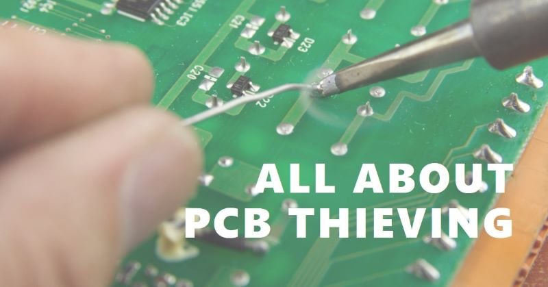
What is PCB thieving?
Understanding PCB thieving is essential for anyone involved in the design and manufacturing of PCBs. By appreciating its importance and function, designers can make informed decisions that contribute to the production of high-quality, reliable PCBs. In the following sections, we will delve deeper into the specific techniques and best practices for implementing PCB thieving effectively.
What is Thieving in PCB?
PCB thieving, also referred to as copper thieving or copper balancing. It is a technique used in PCB manufacturing to address issues related to uneven copper distribution on the PCB surface. During the PCB fabrication process, copper is typically deposited or plated onto the substrate to create conductive traces, pads and other features required for electronic circuitry. However, variations in the distribution of copper across the PCB surface can lead to several undesirable outcomes, including:
- Uneven Plating: Variations in copper thickness can occur due to factors such as uneven surface topography, varying current densities during electroplating or localized substrate properties. This can result in regions of the PCB having thicker or thinner copper layers than desired, leading to inconsistent electrical performance and reliability.
- Copper Thieving: In areas where copper deposition is excessive, known as “copper islands,” excessive copper may need to be removed to achieve the desired copper thickness across the PCB. This process of selectively removing excess copper, often through etching or milling techniques, which is referred to as copper thieving. Copper thieving helps balance the copper distribution on the PCB surface and ensures uniform electrical characteristics and impedance matching across the circuit.
- Warpage and Dimensional Stability: Non-uniform copper distribution can also contribute to PCB warpage or dimensional instability during manufacturing processes such as solder reflow. Variations in copper thickness can lead to differential thermal expansion and contraction across the PCB, resulting in bowing, twisting or distortion of the board. This can affect the accuracy of component placement, solder joint quality and overall reliability of the electronic system.
How to Mitigate PCB Thieving?
To address the challenges associated with PCB thieving and ensure the integrity and reliability of PCB manufacturing processes, several strategies and best practices can be employed:
- Design Optimization: PCB designers can optimize the layout and placement of copper features to minimize variations in copper distribution across the PCB surface. This may involve adjusting trace widths, pad sizes and copper pour areas to achieve more uniform copper thickness and distribution.
- Copper Balancing Techniques: PCB manufacturers can implement copper balancing techniques during the fabrication process to achieve more consistent copper thickness across the PCB surface. This may include adjusting plating parameters, using specialized plating processes or incorporating copper thieving patterns into the PCB layout to redistribute excess copper more effectively.
- Advanced Manufacturing Processes: Leveraging advanced manufacturing technologies and equipment can help improve the accuracy, precision and repeatability of PCB fabrication processes. This includes using automated equipment for copper deposition, etching and milling, as well as employing advanced inspection and quality control measures to detect and correct variations in copper distribution early in the manufacturing process.
- Material Selection: Choosing high-quality substrate materials with uniform electrical and mechanical properties can help minimize variations in copper distribution and improve overall PCB performance and reliability. Additionally, selecting substrate materials with low coefficient of thermal expansion (CTE) can reduce the risk of warpage and dimensional instability during assembly and operation.
Challenges and Best Practices in PCB Thieving
PCB thieving, while beneficial, presents several challenges that manufacturers must navigate to achieve optimal outcomes. One of the primary challenges lies in the design limitations that can arise when integrating thieving patterns into printed circuit boards (PCBs). These patterns are essential for maintaining uniform copper distribution during the electroplating process, but improper placement or design can lead to undesirable effects, such as signal interference or increased production costs.
Another significant challenge is the expertise required to effectively place thieving patterns. This process demands a deep understanding of the PCB’s design and the electroplating process. Without this knowledge, there’s a risk of negatively impacting the board’s electrical performance or structural integrity. Consequently, investing in training and hiring skilled professionals who can navigate these complexities is crucial for manufacturers.
To overcome these challenges, implementing best practices in PCB thieving is essential. One critical best practice is to consider design constraints early in the development process. By integrating thieving patterns into the initial design phase, manufacturers can avoid costly redesigns and ensure that the patterns are optimally placed. Utilizing advanced software tools can also significantly aid in this process, as they can automatically suggest thieving pattern placements based on the board’s design and electroplating requirements.
Collaboration between design and manufacturing teams is another key best practice. Effective communication ensures that the thieving patterns meet both design specifications and manufacturing capabilities. Regular meetings and collaborative tools can facilitate this communication, enabling teams to address potential issues before they arise.
Moreover, keeping up-to-date with industry standards and emerging technologies can provide manufacturers with new strategies and tools for effective PCB thieving. Continuous learning and adaptation are vital in this ever-evolving field, ensuring that manufacturers can produce high-quality PCBs while minimizing potential issues related to copper distribution and electroplating.
Conclusion
In Conclusion, PCB thieving represents a critical consideration in ensuring the reliability, performance and quality of electronic systems. By understanding the concept of PCB thieving and implementing effective strategies for mitigating its effects, PCB designers and manufacturers can achieve more consistent copper distribution, improve electrical performance, and enhance the reliability of PCBs for a wide range of applications and industries.
By paying attention to these details and employing best practices, the complex process of PCB manufacturing can be optimized to produce superior electronic products that meet the high standards of today’s technology-driven world.