Understanding Radiation Loss: Its Impact on PCB Circuit Performance and Mitigation Strategies
In the realm of printed circuit board (PCB) design and manufacturing, radiation loss is a phenomenon that can significantly impact the performance and efficiency of electronic circuits. As electronic devices become more compact and operate at higher frequencies, the effects of radiation loss become increasingly relevant. This comprehensive article aims to provide a deep understanding of radiation loss, its causes, and its impact on PCB circuit performance.
What is Radiation Loss?
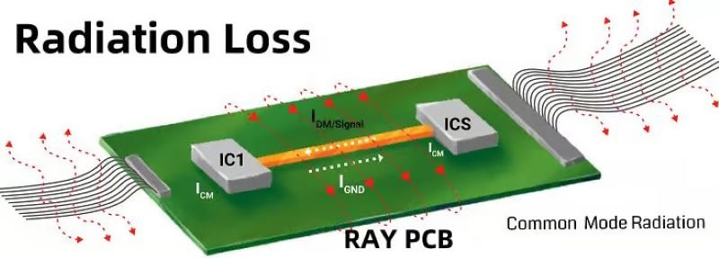
Radiation loss, also known as electromagnetic radiation or electromagnetic interference (EMI), refers to the unintended emission of electromagnetic energy from conductors on a PCB. This energy is radiated into the surrounding environment and can potentially interfere with other electronic devices or systems.
When an alternating current flows through a conductor, such as a trace on a PCB, it generates an electromagnetic field around the conductor. This field can induce currents in nearby conductors, causing interference and potentially affecting the performance of the circuit. The intensity and distribution of the radiated energy depend on various factors, including the frequency of the signal, the physical layout of the PCB, and the materials used in its construction.
Causes of Radiation Loss
There are several factors that contribute to radiation loss in PCB circuits:
- High-Frequency Signals As the operating frequency of electronic circuits increases, the wavelength of the signals becomes shorter, making them more susceptible to radiation loss. At high frequencies, the electromagnetic fields generated by the conductors become more intense, leading to increased radiation.
- Discontinuities and Impedance Mismatches Discontinuities in the PCB layout, such as bends, vias, or abrupt changes in trace width, can cause impedance mismatches and reflections. These discontinuities act as antennas, radiating electromagnetic energy and contributing to radiation loss.
- Improper Grounding and Shielding Inadequate grounding or shielding can exacerbate radiation loss by allowing electromagnetic fields to escape from the PCB and interact with other components or systems. Proper grounding and shielding techniques are crucial for minimizing radiation loss.
- Material Properties The properties of the materials used in PCB construction, such as the dielectric constant and loss tangent of the substrate, can influence the propagation of electromagnetic waves and contribute to radiation loss.
Impact of Radiation Loss on PCB Circuit Performance
Radiation loss can have several detrimental effects on the performance of PCB circuits, including:
- Signal Integrity Issues Radiation loss can lead to signal degradation, crosstalk, and interference between different circuits or components on the PCB. This can result in data errors, reduced signal-to-noise ratio, and overall performance degradation.
- Electromagnetic Compatibility (EMC) Concerns Excessive radiation from a PCB can interfere with other electronic devices or systems in the vicinity, causing electromagnetic compatibility (EMC) issues. This can lead to regulatory compliance problems and potential legal implications.
- Power Loss and Efficiency Reduction Radiation loss can result in a portion of the signal power being dissipated into the environment, reducing the overall efficiency of the circuit and potentially affecting its power consumption and heat dissipation characteristics.
- Increased Susceptibility to External Interference Circuits with high levels of radiation loss may also be more susceptible to external electromagnetic interference, further compromising their performance and reliability.
Mitigating Radiation Loss in PCB Design
To minimize the impact of radiation loss and improve the performance of PCB circuits, designers can implement various strategies and techniques:
- Proper Layout and Routing Careful layout and routing of traces, components, and power planes can help reduce discontinuities and impedance mismatches, thereby minimizing radiation loss. Techniques such as maintaining consistent trace widths, avoiding sharp bends, and implementing appropriate spacing between traces can be employed.
- Shielding and Grounding Incorporating proper shielding and grounding techniques is crucial for containing electromagnetic fields and preventing radiation loss. This can include the use of ground planes, shielding enclosures, or dedicated grounding layers.
- Material Selection Choosing PCB materials with appropriate dielectric properties and low loss tangents can help reduce the propagation of electromagnetic waves and minimize radiation loss.
- Impedance Matching Ensuring impedance matching throughout the PCB circuit can minimize reflections and reduce radiation loss. This can be achieved through careful trace and component layout, as well as the use of termination resistors or other impedance matching techniques.
- Filtering and Suppression Implementing filtering and suppression techniques, such as the use of ferrite beads or decoupling capacitors, can help reduce high-frequency noise and mitigate radiation loss.
Conclusion
In conclusion, Radiation loss is a critical consideration in PCB circuit design, particularly as operating frequencies and device densities continue to increase. Understanding the causes and effects of radiation loss is essential for ensuring optimal circuit performance, electromagnetic compatibility, and regulatory compliance. By implementing appropriate mitigation strategies, such as proper layout and routing, shielding and grounding, material selection, impedance matching, and filtering techniques, designers can minimize radiation loss and enhance the overall performance and reliability of their PCB circuits.