
Step-by-Step Guide to Programming a 4-Bit Adder in Verilog
Verilog is a widely-used hardware description language (HDL) for designing digital circuits and systems. It allows designers to model and simulate hardware behavior at various levels of abstraction, from gate-level to system-level. One common use of Verilog is designing arithmetic circuits like adders, which are fundamental components in processors and digital systems.
A 4-bit adder is a digital circuit that performs addition on two 4-bit binary numbers, producing a 4-bit sum and a carry-out bit. Understanding how to program a 4-bit adder in Verilog is a foundational step for anyone diving into digital design. This article walks you through the concepts, design process, and Verilog implementation of a 4-bit adder, using a modular and systematic approach.
Understanding the Basics
What is a 4-bit Adder?
A 4-bit adder performs binary addition of two 4-bit inputs, producing a sum output and a carry-out bit. It can be constructed by cascading four full adders, where each full adder handles one bit of the inputs, along with the carry from the previous stage.
- Concept of Binary Addition
Binary addition operates like decimal addition but with only two digits: 0 and 1. The key rules are:- 0 + 0 = 0
- 0 + 1 = 1
- 1 + 0 = 1
- 1 + 1 = 10 (0 with a carry of 1)
- Ripple Carry Adder
A ripple carry adder is a type of adder where the carry output of one full adder is connected to the carry input of the next full adder in the chain. The term “ripple” refers to the sequential propagation of the carry through each adder, which can cause a delay in the final output.
Key Components in Verilog
To design a 4-bit adder, understanding the following Verilog constructs is essential:
- Modules
Modules are the building blocks of Verilog designs. Each module defines a specific functionality and can be reused in larger designs. - Inputs and Outputs
Verilog modules useinputandoutputkeywords to define ports. These are used to interact with external signals or other modules. - Behavioral vs. Structural Modeling
- Behavioral Modeling: Describes the functionality of a circuit using high-level constructs like
alwaysblocks. - Structural Modeling: Represents the circuit at a lower level, connecting components (e.g., gates or modules) to mimic hardware implementation.
- Behavioral Modeling: Describes the functionality of a circuit using high-level constructs like
Designing the 4-Bit Adder
Truth Table for Addition
The core of a 4-bit adder is the full adder. A full adder takes three inputs (two operand bits and a carry-in) and produces two outputs (sum and carry-out).
| A | B | Cin | Sum | Cout |
|---|---|---|---|---|
| 0 | 0 | 0 | 0 | 0 |
| 0 | 0 | 1 | 1 | 0 |
| 0 | 1 | 0 | 1 | 0 |
| 0 | 1 | 1 | 0 | 1 |
| 1 | 0 | 0 | 1 | 0 |
| 1 | 0 | 1 | 0 | 1 |
| 1 | 1 | 0 | 0 | 1 |
| 1 | 1 | 1 | 1 | 1 |
This truth table is the basis for constructing the logic of a full adder.
Block Diagram
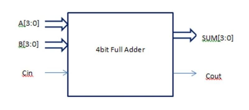
A 4-bit adder consists of four full adders connected in series. Each full adder computes the sum and carry for one bit, with the carry-out of each stage fed into the carry-in of the next stage.
- Inputs: Two 4-bit numbers (
A[3:0]andB[3:0]) and an initial carry-in (Cin). - Outputs: A 4-bit sum (
Sum[3:0]) and a carry-out (Cout).
The block diagram includes:
- Four full adders labeled FA0 (least significant bit) to FA3 (most significant bit).
- Carry propagation from one stage to the next.
Step-by-Step Design Approach
- Design a Full Adder Module
- Create a Verilog module for a single full adder.
- Inputs:
A,B, andCin. - Outputs:
SumandCout. - Implement using behavioral (e.g., with
assign) or structural modeling.
- Combine Full Adders to Form a 4-Bit Adder
- Create a top-level module for the 4-bit adder.
- Instantiate four full adder modules.
- Connect the carry-out of each stage to the carry-in of the next stage.
- Test and Verify
- Write a testbench to verify the functionality of both the full adder and 4-bit adder.
- Simulate using appropriate tools to ensure correctness.
By following this step-by-step process, you can efficiently design a functional 4-bit adder in Verilog.
Verilog Implementation
Full Adder Module
Below is the Verilog code for a single full adder:
module full_adder (
input A, // First operand bit
input B, // Second operand bit
input Cin, // Carry-in
output Sum, // Sum output
output Cout // Carry-out
);
// Logic for sum and carry-out
assign Sum = A ^ B ^ Cin; // XOR operation for sum
assign Cout = (A & B) | (B & Cin) | (A & Cin); // OR operation for carry-out
endmodule
Explanation:
- The
assignstatements implement the logic equations for the sum and carry-out. - The module is parameterized with
inputandoutputports, making it reusable for other designs.
4-Bit Adder Module
The 4-bit adder is built by instantiating four full adders:
module adder_4bit (
input [3:0] A, // 4-bit input A
input [3:0] B, // 4-bit input B
input Cin, // Carry-in
output [3:0] Sum, // 4-bit Sum output
output Cout // Final Carry-out
);
wire [3:0] Carry; // Intermediate carry signals

// Instantiate four full adders
full_adder FA0 (.A(A[0]), .B(B[0]), .Cin(Cin), .Sum(Sum[0]), .Cout(Carry[0]));
full_adder FA1 (.A(A[1]), .B(B[1]), .Cin(Carry[0]), .Sum(Sum[1]), .Cout(Carry[1]));
full_adder FA2 (.A(A[2]), .B(B[2]), .Cin(Carry[1]), .Sum(Sum[2]), .Cout(Carry[2]));
full_adder FA3 (.A(A[3]), .B(B[3]), .Cin(Carry[2]), .Sum(Sum[3]), .Cout(Cout));

endmodule
Explanation:
- The
wiredata type connects the carry-out of one full adder to the carry-in of the next. - The top-level module encapsulates the design and connects all components.
Simulation and Testing
Testbench for the 4-Bit Adder
A testbench simulates and verifies the behavior of a design. It provides input signals and checks the outputs against expected values.
module tb_adder_4bit;
reg [3:0] A, B; // 4-bit inputs
reg Cin; // Carry-in
wire [3:0] Sum; // 4-bit sum output
wire Cout; // Carry-out

// Instantiate the 4-bit adder
adder_4bit DUT (.A(A), .B(B), .Cin(Cin), .Sum(Sum), .Cout(Cout));

initial begin
// Test Cases
$monitor("Time=%0t: A=%b, B=%b, Cin=%b -> Sum=%b, Cout=%b", $time, A, B, Cin, Sum, Cout);

// Test case 1
A = 4'b0001; B = 4'b0010; Cin = 0; #10;
// Test case 2
A = 4'b1010; B = 4'b0101; Cin = 1; #10;
// Test case 3
A = 4'b1111; B = 4'b1111; Cin = 0; #10;

$stop;
end
endmodule
Explanation:
- The
initialblock defines input sequences and test cases. - The
$monitorstatement prints input and output values during simulation. - The testbench ensures the adder performs correctly for various input combinations.
Simulation Results
To simulate:
- Use a tool like ModelSim, Vivado, or any Verilog simulator.
- Compile the Verilog files and run the testbench.
- Observe the waveform or console outputs to verify correctness.
Expected Outputs:
- For
A = 4'b0001, B = 4'b0010, Cin = 0, expectSum = 4'b0011, Cout = 0. - For
A = 4'b1010, B = 4'b0101, Cin = 1, expectSum = 4'b0000, Cout = 1. - For
A = 4'b1111, B = 4'b1111, Cin = 0, expectSum = 4'b1110, Cout = 1.
Optimizing the Design
- Speed Optimization
- Replace ripple carry with a carry-lookahead adder for faster computation.
- Use pipelining to handle larger bit widths efficiently.
- Resource Optimization
- Use Verilog’s arithmetic operators (
+) instead of manually instantiating adders: assign {Cout, Sum} = A + B + Cin; - This approach is concise and leverages built-in synthesis optimizations.
- Use Verilog’s arithmetic operators (
- Alternate Methods
- Explore behavioral modeling for more complex arithmetic operations.
Conclusion
In conclusion, Designing a 4-bit adder in Verilog is an excellent way to understand digital logic, modular design, and the power of hardware description languages. This article covered:
- Full adder design and cascading to form a 4-bit adder.
- Writing Verilog code for modular and hierarchical designs.
- Simulating and testing the design to ensure correctness.