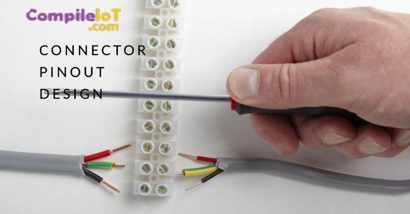
How to Design a Connector Pinout For Your PCB?
Designing a connector pinout for your PCB requires careful consideration of the connector type, pin functions, layout and testing. By following the steps outlined in this article, you can create an effective and reliable connector pinout design that ensures seamless communication between your PCB and external devices or components.
Remember, a well-designed connector pinout not only enhances the functionality of your PCB but also improves the overall user experience. Take the time to understand the requirements and constraints of your project and design a connector pinout that meets your specific needs.
What is Connector Pinout Design?
Connector pinout design refers to the arrangement and assignment of pins or terminals on a connector. A connector is a device used to establish a physical and electrical connection between two or more electronic components or devices. The pinout design determines how the pins or terminals are organized and what signals or functions they carry.
Factors to Consider in Connector Pinout Design
When designing a connector pinout, several factors need to be taken into account:
- Functionality: The primary consideration in pinout design is the intended functionality of the connector. Each pin should be assigned a specific function, such as power supply, data transmission or control signals. The pinout design should ensure that the necessary signals are available and properly routed.
- Compatibility: The pinout design should be compatible with the devices or components that will be connected using the connector. It should adhere to industry standards and specifications to ensure compatibility with a wide range of devices.
- Signal Integrity: Signal integrity refers to the quality and reliability of signals transmitted through the connector. The pinout design should minimize signal degradation, noise, and interference. Proper consideration should be given to signal grounding, shielding and impedance matching to maintain signal integrity.
- Physical Constraints: The physical constraints of the connector and the available space for pins should also be considered. The pinout design should take into account the size, shape and orientation of the connector which ensures that the pins can be easily accessed and connected without any physical obstructions.
- Future Expansion: It is important to consider future expansion or modifications when designing a pinout. Leaving room for additional pins or functions can allow for future upgrades or compatibility with new technologies. This can help extend the lifespan and versatility of the connector.
Tools and Techniques for Connector Pinout Design
Several tools and techniques are available to assist in the design of connector pinouts:
1. CAD Software:
Computer-aided design (CAD) software provides a comprehensive platform for designing and visualizing connector pinouts. CAD tools allow engineers to create accurate and detailed pinout diagrams, specifying the functions and assignments of each pin. This helps in ensuring proper connectivity and compatibility.
2. Pinout Diagrams:
Pinout diagrams are graphical representations of connector pin assignments. These diagrams provide a clear and concise overview of the pinout design, making it easier to understand and implement. Pinout diagrams can be created using software tools or drawn manually.
3. Signal Mapping and Testing:
Signal mapping involves mapping the signals or functions to be transmitted through the pins. This helps in identifying potential conflicts or issues in the pinout design. Additionally, testing the pinout design using signal generators and oscilloscopes can validate the functionality and integrity of the connector.
Connector pinout design refers to the arrangement and configuration of pins within a connector. Each pin serves a specific purpose and is responsible for carrying a particular signal or providing power to the connected device.
Step-by-Step Guide to Designing a Connector Pinout
The pinout determines how the electrical connections are made between the PCB and external devices or components. It is essential to design the connector pinout carefully to ensure proper functionality and compatibility. Let’s explore the step-by-step guide to designing a connector pinout for your PCB.
1. Identify the Connector Type
The first step in designing a connector pinout is to identify the type of connector you will be using. There are various types of connectors available, such as D-sub, USB, HDMI, and RJ45, each with its own pin configuration. Understanding the specific connector type will help you determine the number of pins and their functions.
2. Determine the Pin Functions
Once you have identified the connector type, the next step is to determine the pin functions. Each pin on the connector serves a specific purpose, such as power supply, data transmission or ground connection. It is crucial to carefully review the datasheet or technical specifications of the connector to understand the functions of each pin.
Assigning the correct functions to the pins ensures that the PCB can communicate effectively with the external devices or components. It also helps prevent any potential damage or short circuits that may occur if the pins are incorrectly connected.
3. Plan the Pinout Layout
After determining the pin functions, it is time to plan the pinout layout on your PCB. The pinout layout refers to the physical arrangement of the pins on the PCB. Consider the following factors when planning the pinout layout:
- Signal Integrity: Place pins that carry high-frequency signals away from pins that carry low-frequency signals to minimize interference.
- Power and Ground: Group power and ground pins together to ensure a stable power supply and reduce noise.
- Logical Order: Arrange the pins in a logical order that makes it easier for users to connect external devices or components.
- Space Constraints: Consider the available space on your PCB and ensure that the connector pinout fits within the designated area.
4. Create a Pinout Diagram
Creating a pinout diagram is a helpful visual representation of your connector pinout design. It allows you to easily reference the pin functions and their physical locations on the PCB. You can use software tools like EAGLE, Altium Designer or even basic drawing software to create your pinout diagram.
Include labels and descriptions for each pin to provide clear instructions for users. Additionally, you can color-code or use different line styles to differentiate between power, ground, and signal pins, making it even more user-friendly.
5. Test and Verify
Before finalizing your connector pinout design, it is crucial to test and verify its functionality. Connect the PCB to the external devices or components using the designed pinout and ensure that the expected connections are established. Use a multimeter or oscilloscope to check for proper voltage levels, signal integrity, and continuity.
If any issues or inconsistencies are identified during testing, revisit the pinout design and make the necessary adjustments. It is essential to iterate and refine the design until the desired functionality is achieved.
The Importance of Connector Pinout Design
The pinout design of a connector is essential for several reasons:
1. Compatibility and Interoperability
A well-designed pinout ensures compatibility and interoperability between different devices and systems. By following industry standards and guidelines, manufacturers can ensure that their connectors can be used with a wide range of devices, regardless of the brand or model.
For example, USB connectors have a standardized pinout design, which allows USB cables to be used with various devices such as computers, smartphones, printers, and more. This standardization simplifies the process of connecting devices and eliminates the need for device-specific cables.
2. Signal Integrity
The pinout design also plays a crucial role in maintaining signal integrity. Each pin is responsible for carrying a specific signal, such as data, power, or audio. A well-designed pinout minimizes signal interference and ensures that the intended signals are transmitted accurately.
Signal integrity is particularly important in high-speed data transmission applications, such as HDMI or Ethernet connections. A poorly designed pinout can result in signal degradation, leading to data loss, poor audio/video quality, or even device malfunction.
3. Ease of Use
A well-designed pinout makes it easier for users to connect and disconnect devices. By following intuitive pinout configurations, manufacturers can ensure that users can easily identify the correct pins and establish a secure connection without the risk of damaging the devices.
For example, audio connectors often follow a color-coded pinout design, where the green pin is designated for audio output, the pink pin for microphone input, and the blue pin for line input. This color-coding simplifies the process of connecting speakers, headphones, or microphones to audio devices.
Conclusion
In conclusion, Connector pinout design is a critical aspect of electronic system design. It ensures proper connectivity, functionality, and compatibility between different components and devices. By considering factors such as functionality, compatibility, signal integrity, physical constraints, and future expansion, engineers can create effective and reliable pinout designs. Utilizing tools and techniques such as CAD software, pinout diagrams and signal mapping helps streamline the design process and minimize errors. With a well-designed pinout, electronic systems can operate efficiently and reliably.