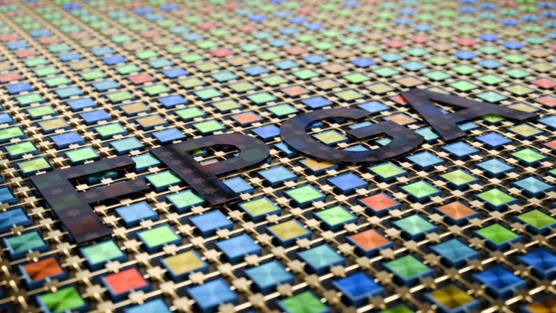
FPGA Design: Architecture, Programming and Applications
Field Programmable Gate Arrays (FPGAs) are versatile, reprogrammable silicon chips that have revolutionized modern digital system design. Unlike traditional hardware solutions, FPGAs offer a unique combination of hardware performance and software flexibility, making them indispensable in applications ranging from telecommunications to artificial intelligence. This article explores the architecture of FPGAs, detailing their components and functionality, to provide a clear understanding of how they enable cutting-edge technological advancements.
What is an FPGA?
An FPGA is a semiconductor device that can be configured by the user after manufacturing, hence the term “field-programmable.” Unlike fixed-function Application-Specific Integrated Circuits (ASICs), FPGAs allow developers to define their functionality through a hardware description language (HDL), such as VHDL or Verilog. This configurability makes FPGAs highly adaptable to a variety of tasks.
Comparison with Other Programmable Devices
- CPUs (Central Processing Units):
- CPUs are general-purpose processors designed to execute sequential instructions. While they are flexible and easy to program, they often struggle to achieve high performance for computationally intensive tasks.
- GPUs (Graphics Processing Units):
- GPUs are specialized for parallel computations, particularly in graphics rendering and AI workloads. However, their architecture is fixed, limiting adaptability to non-graphics-specific applications.
- FPGAs:
- Unlike CPUs and GPUs, FPGAs provide hardware-level parallelism and can be tailored to specific applications. This allows them to outperform CPUs and GPUs in latency-sensitive or power-constrained environments.
Key Advantages of FPGAs
- Flexibility: Programmable nature allows reconfiguration for various applications.
- Parallelism: Ability to execute multiple operations simultaneously at the hardware level.
- Low Latency: Optimized for real-time processing tasks.
- Energy Efficiency: Custom designs often consume less power than CPUs or GPUs for equivalent tasks.
- Scalability: Suitable for both prototyping and large-scale deployment.
Overview of FPGA Architecture
General Structure of an FPGA
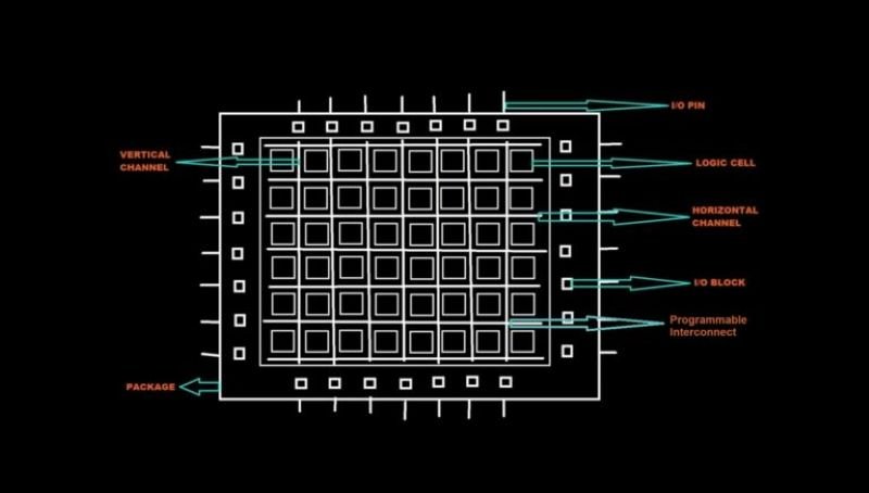
An FPGA is organized into a grid-like structure containing logic blocks, interconnects, and input/output elements. These components work together to implement the desired hardware functionality. The flexibility of this architecture allows FPGAs to support complex, high-speed designs.
Explanation of the Primary Components
- Configurable Logic Blocks (CLBs):
- CLBs are the core computational elements of an FPGA. Each CLB typically contains Look-Up Tables (LUTs), flip-flops, and multiplexers. LUTs implement combinational logic, while flip-flops store state information. Together, these elements enable a wide range of digital functions.
- Interconnects (Routing Fabric):
- Interconnects form the programmable wiring that connects CLBs, I/O blocks, and other resources within the FPGA. These connections are controlled by switch matrices, allowing signals to route efficiently across the chip.
- Input/Output Blocks (IOBs):
- IOBs manage the interaction between the FPGA and external devices. They support various standards and protocols, ensuring compatibility with diverse systems.
- Clock Management:
- Clock signals synchronize operations within the FPGA. Dedicated resources like Phase-Locked Loops (PLLs) and Clock Management Tiles (CMTs) provide precise control over clock generation and distribution, enabling high-performance designs.
Key Components of FPGA Architecture
4.1 Configurable Logic Blocks (CLBs)
- Composition and Functionality: CLBs consist of Look-Up Tables (LUTs), flip-flops, and multiplexers. LUTs implement combinational logic, while flip-flops store and manage sequential logic states.
- Look-Up Tables (LUTs): Act as small memory arrays that provide pre-computed logic values based on input combinations.
- Flip-Flops and Registers: Used for state retention and synchronization of logic operations.
4.2 Routing Interconnects
- Switch Matrices and Programmable Interconnects: Enable dynamic connectivity between CLBs and other components. Switch matrices provide flexible routing paths.
- Hierarchical Routing Structure: Ensures efficient signal propagation across the FPGA, balancing speed and resource utilization.
4.3 Input/Output Blocks (IOBs)
- Role in Connecting FPGAs to External Devices: IOBs serve as interfaces for data exchange between the FPGA and peripheral devices or systems.
- Configurable IO Standards: Support a wide range of communication protocols and voltage levels, enhancing compatibility and functionality.
4.4 Embedded Memory Blocks
- Types of Memory: FPGAs include various memory types such as Block RAM (BRAM), Distributed RAM, and external memory interfaces like DRAM or SRAM.
- Usage in Buffering and Storage: Memory blocks are crucial for data storage, buffering, and facilitating high-speed computations.
4.5 Specialized Resources
- DSP Slices for Arithmetic Operations: Provide dedicated hardware for complex mathematical operations, optimizing performance for signal processing tasks.
- Embedded Processors and Soft Cores: Include on-chip processors or allow implementation of custom soft processors for hybrid processing.
- High-Speed Transceivers: Enable high-bandwidth communication for networking and data transfer applications.
FPGA Programming and Configuration
- Bitstream Generation: A bitstream file defines the FPGA’s configuration. It is generated during the design process and loaded into the FPGA to implement the desired functionality.
- Configuration Modes:
- JTAG: Used for debugging and direct configuration.
- Serial: Enables configuration through serial protocols.
- Parallel: Provides faster configuration speeds for large designs.
- Reconfiguration and Partial Reconfiguration: FPGAs can be reprogrammed entirely or partially, allowing dynamic updates to specific sections of the chip without disrupting ongoing operations.
Design Flow in FPGA Development
Steps Involved in FPGA Design:
- Design Entry: Create the design using Hardware Description Languages (HDLs) or graphical tools.
- Synthesis: Convert HDL code into a netlist representing the logical elements of the design.
- Place-and-Route: Map the design onto FPGA resources and optimize placement for performance.
- Timing Analysis: Ensure the design meets timing requirements to avoid errors in operation.
Tools and Software:
- Vivado (Xilinx): Comprehensive design suite for Xilinx FPGAs.
- Quartus (Intel): Design and analysis software for Intel FPGAs.
- Libero (Microsemi): Tools for Actel/Microsemi FPGAs.
FPGA Applications and Use Cases
Telecommunications and Networking:
FPGAs are used in high-speed communication systems for packet processing, signal modulation, and error correction.
Signal Processing:
Ideal for audio, video, and radar signal processing due to their parallel processing capabilities.
Artificial Intelligence and Machine Learning:
Used for accelerating neural networks and inference engines in edge and cloud-based AI systems.
Automotive and Aerospace Systems:
Support advanced driver-assistance systems (ADAS), avionics, and real-time control systems with high reliability and low latency.
Future Trends in FPGA Architecture
- Heterogeneous Integration: The incorporation of multiple technologies, such as CPUs, GPUs, and AI accelerators, on a single FPGA chip to enhance versatility and performance.
- Advancements in Silicon Technology: Utilization of smaller process nodes (e.g., 7nm, 5nm) to improve power efficiency, reduce cost, and increase logic density.
- AI and ML Optimization: Development of FPGA architectures tailored for AI workloads, with dedicated resources for neural networks and deep learning models.
- Dynamic Partial Reconfiguration: Improved capabilities for real-time, on-the-fly updates to portions of the FPGA without halting operations.
- Cloud Integration: Expansion of FPGA-as-a-Service (FaaS) platforms, enabling seamless deployment of FPGA designs in cloud computing environments.
Conclusion
In conclusion, Field Programmable Gate Arrays have emerged as a cornerstone of modern digital design, offering unmatched flexibility, performance, and scalability. Their ability to adapt to diverse applications—from telecommunications to artificial intelligence—makes them a critical technology in the evolving landscape of computing. With continuous advancements in architecture and integration, FPGAs are poised to remain at the forefront of innovation, shaping the future of technology for years to come.