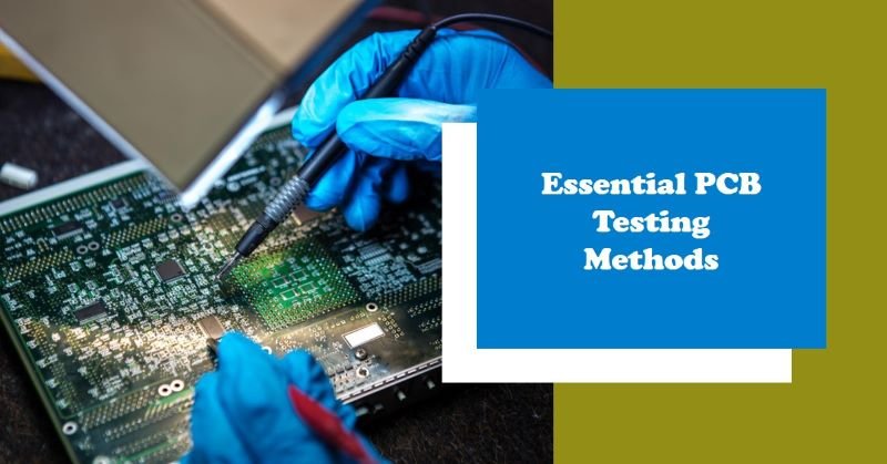
Essential PCB Testing Methods
Printed Circuit Board (PCB) testing is a critical step in ensuring that a design works as expected before moving into mass production. Proper testing helps catch defects, inconsistencies, and potential issues that could compromise the functionality of the entire system. Without thorough testing, a seemingly minor defect can cause failures, leading to costly rework or even damage to connected devices. This article outlines the essential steps to test a PCB effectively, covering visual inspection, continuity testing, power-on testing, functional testing, and signal integrity checks.
1. Visual Inspection
Visual inspection is the first step in testing a PCB and helps identify physical defects before powering on the board. This simple but effective method involves checking the PCB’s surface for any obvious issues, such as missing components or poorly soldered joints.
Why visual inspection is important: Detecting obvious physical defects
A thorough visual inspection can quickly reveal common issues like misaligned components, cold solder joints, or cracked traces that may have occurred during the assembly process. Identifying these defects early on helps avoid further complications when powering the board for functional testing.
What to check: Missing components, soldering errors, cracked traces, and misalignments
- Missing components: Ensure that all components specified in the Bill of Materials (BOM) are present on the board.
- Soldering errors: Look for cold or bridged solder joints that could cause shorts or open circuits.
- Cracked traces: Verify that PCB traces are intact and not broken or damaged.
- Misalignments: Ensure that components like ICs and connectors are correctly aligned in their designated positions.
Tools for visual inspection: Magnifying glasses, microscopes
To conduct a detailed inspection, basic tools like magnifying glasses or microscopes can be used to zoom in on specific areas of the PCB. In advanced cases, Automated Optical Inspection (AOI) systems may be employed for mass production lines, but for initial testing, manual inspection is usually sufficient.
2. Continuity Testing
After visual inspection, continuity testing is used to ensure that all the electrical connections on the PCB are properly established. This test checks if the circuit pathways are complete, preventing issues like open circuits that would stop the board from functioning.
Purpose: Ensure that all connections are electrically continuous
Continuity testing helps identify broken traces, poor solder joints, or any disconnections that can occur during manufacturing. This step verifies the integrity of the electrical connections between components and traces.
Tools used: Multimeter (set to continuity mode)
A multimeter set to continuity mode is commonly used to perform this test. When the probes touch two points of a connection, the multimeter will emit a sound or display a value, indicating that the connection is continuous.
How to perform: Testing traces, vias, and connections for proper electrical pathways
- Place the multimeter’s probes at two ends of a trace or component pin.
- If the multimeter beeps or shows a reading, the connection is intact.
- Test traces, vias (vertical interconnect access), and components in this manner to ensure all pathways are electrically connected.
3. Power-on Testing
Power-on testing is a critical step that involves applying power to the PCB to test its voltage levels and current consumption. Before applying power, it’s essential to verify that the board does not have short circuits, incorrect connections, or reversed polarity, as these could result in damage.
Before powering on: Double-check for short circuits, wrong connections, or reversed polarity
Before powering the board, perform a final check for shorts between power and ground, as well as ensuring the proper orientation of components like diodes and capacitors. Ensuring these components are correctly installed helps prevent catastrophic damage when power is applied.
Testing procedure: Apply power and check voltage levels across critical points
- Power up the PCB using a regulated power supply.
- Measure the voltage across critical points such as the power supply pins, ICs, and key components to ensure they are within the expected range.
- Monitor the current drawn by the board to ensure it is within safe limits for the circuit.
Safety tips: Use current-limiting power supplies to avoid damage during the initial power-up
To prevent overcurrent or overheating, use a current-limiting power supply. This precaution limits the current during the initial power-up phase and can help prevent damage in case there are shorts or incorrect connections.
4. Functional Testing
Functional testing evaluates whether the PCB performs its intended functions correctly. At this stage, the behavior of key components such as microcontrollers, sensors, and LEDs is tested to verify that the board is operating as designed.
Objective: Ensure the PCB performs its intended function
This test ensures that the circuit performs according to its design, validating that all components are functioning properly and responding to input signals or conditions.
Testing key components and circuits (e.g., microcontrollers, sensors, LEDs)
- Test microcontrollers for proper boot-up and functionality.
- Verify sensor data is being correctly read and processed.
- Check the operation of any visible indicators, such as LEDs, to ensure they respond as expected.
Using oscilloscopes and logic analyzers to verify signal integrity and timing
To test high-speed or complex circuits, tools like oscilloscopes and logic analyzers are used to measure voltage signals and verify their accuracy over time. These tools help identify timing issues, noise, or signal degradation that may affect performance.
5. Signal Integrity Testing
Signal integrity testing focuses on verifying the quality of electrical signals as they pass through the PCB’s traces. This is especially important for high-speed designs where signal distortion or noise can significantly impact performance.
Purpose: Check signal quality and performance
Signal integrity testing ensures that signals maintain their expected shape and timing as they travel across the PCB without interference, reflection, or loss.
Common tools: Oscilloscopes, signal generators
Oscilloscopes are used to visualize the electrical signals, while signal generators can create specific test signals to verify the PCB’s response.
Testing procedure: Look for signal distortion, noise, and reflections on high-speed traces
- Use an oscilloscope to measure key signals, checking for distortion, excessive noise, or reflections.
- On high-speed designs, verify that transmission lines are properly terminated to minimize reflections.
- Evaluate the overall signal quality to ensure reliable communication between components.
6. In-Circuit Testing (ICT)
In-Circuit Testing (ICT) is a widely used method in PCB testing for automatically verifying the correctness of component placement and identifying issues like shorts or open circuits. ICT offers a more efficient way to test boards, especially in high-volume production environments.
What is ICT: Automated testing for component placement, shorts, and opens
ICT involves using a test fixture known as a “bed of nails,” which connects to various points on the PCB to check components, connections, and the overall integrity of the board. It can identify misplaced components, detect shorts between pins, and verify proper solder connections.
Benefits: Faster and more comprehensive testing for large batches
ICT is highly efficient, particularly when testing large quantities of PCBs. The automated nature of ICT allows for rapid testing of each board, ensuring all components are correctly placed and functional. It provides comprehensive testing, covering everything from component value checks to more complex circuit functions.
Limitations: Requires a bed-of-nails test fixture or similar testing hardware
One downside of ICT is that it requires a custom-built test fixture, making it expensive for smaller production runs. The “bed-of-nails” fixture must be tailored to each specific PCB design, and changes to the design can require modifications to the testing setup.
7. Thermal Testing
Thermal testing is crucial for ensuring the PCB can handle the heat generated by its components during operation. Poor heat dissipation can lead to component failure, decreased efficiency, and reduced lifespan of the PCB.
Why thermal testing is important: Ensure proper heat dissipation
Heat buildup in electronic components is inevitable, but managing it effectively is key to preventing damage. Thermal testing helps ensure that the PCB can dissipate heat correctly, keeping temperatures within acceptable limits and avoiding overheating.
How to perform: Thermal imaging or temperature probes to check hotspots
Thermal testing can be performed using thermal imaging cameras or temperature probes. These tools detect hotspots on the PCB, identifying areas where heat accumulates due to inefficient thermal design or malfunctioning components.
What to look for: Overheating components, poor thermal management
During thermal testing, monitor components such as power regulators, processors, and other heat-generating parts. Check for abnormal temperature spikes or hotspots that may indicate poor thermal management. If overheating is detected, consider improving heat sinks, using better thermal interface materials, or revising the PCB layout for better airflow.
8. Environmental Testing
Environmental testing ensures that a PCB can withstand various real-world conditions, such as changes in temperature, humidity, and physical stress. This is especially important for PCBs used in harsh environments like industrial equipment or outdoor applications.
Purpose: Test PCB performance under various conditions (e.g., temperature, humidity)
Environmental tests are designed to replicate the conditions under which the PCB will be used. This includes subjecting the PCB to extreme temperatures, humidity levels, and even physical forces like shock and vibration.
Common tests: Thermal cycling, vibration, and shock testing
- Thermal cycling: Exposes the PCB to extreme temperature changes to test its resistance to expansion and contraction.
- Vibration testing: Simulates the mechanical stress that occurs in moving environments, such as vehicles.
- Shock testing: Tests the PCB’s ability to handle sudden physical impacts.
Importance: Ensuring long-term reliability in real-world applications
By simulating various environmental conditions, these tests help identify weaknesses in the PCB’s design, ensuring that it remains reliable and functional in its intended use cases. Without these tests, the PCB could fail prematurely, leading to costly repairs or replacements.
9. Automated Optical Inspection (AOI)
Automated Optical Inspection (AOI) is a non-contact testing method that uses cameras and image-processing software to inspect PCBs for manufacturing defects. It is commonly used in high-speed production lines to ensure consistency and quality.
What is AOI: Automated systems using cameras to inspect PCBs for defects
AOI systems scan the surface of the PCB with high-resolution cameras, capturing images of the board and comparing them to a known good reference. The system looks for defects such as incorrect component placement, missing parts, and soldering issues.
Advantages: High-speed detection of soldering issues, missing or misplaced components
One of the main advantages of AOI is its speed and accuracy. It can detect a wide range of defects quickly, making it ideal for inspecting PCBs in mass production environments. The system provides detailed feedback on the location and nature of any issues found, allowing for immediate correction.
Applications: Particularly useful in mass production
AOI is highly beneficial in large-scale production runs, where manual inspection would be too slow and error-prone. It ensures a higher level of consistency across multiple boards, reducing the risk of defects reaching the final product.
10. Flying Probe Testing
Flying Probe Testing is a versatile method used to test PCBs without the need for a custom test fixture. This method is suitable for smaller production runs or prototyping, as it is flexible and requires less setup time.
Purpose: Non-contact testing for smaller production runs
Flying probe testing uses multiple movable probes that “fly” over the PCB, making contact with various test points to verify electrical connections. It is ideal for low- to medium-volume production where the cost of a custom test fixture is not justified.
How it works: Probes fly over the board to test for opens, shorts, and component values
The probes make contact with exposed pads, vias, or component leads on the board to check for electrical continuity, shorts, or correct component placement. This method is slower than In-Circuit Testing (ICT) but is more flexible and cost-effective for smaller batches.
Advantages and limitations: Flexible and efficient for low-volume production
The main advantage of flying probe testing is its flexibility, as it does not require a custom fixture. However, it is generally slower than ICT, making it less suitable for high-volume production. It also may not be able to fully test complex, densely packed PCBs as efficiently as ICT.
Conclusion
In summary, PCB testing is an essential process that ensures the quality, reliability, and functionality of the board before it is integrated into a final product. From visual inspection to advanced testing methods like In-Circuit Testing, Thermal Testing, and Signal Integrity Testing, each step plays a critical role in identifying and resolving potential issues. Thorough testing not only improves product performance but also reduces the risk of costly failures in the field, making it an indispensable part of PCB manufacturing. Incorporating these testing methods will ensure that your PCBs meet the highest standards of quality and reliability.
