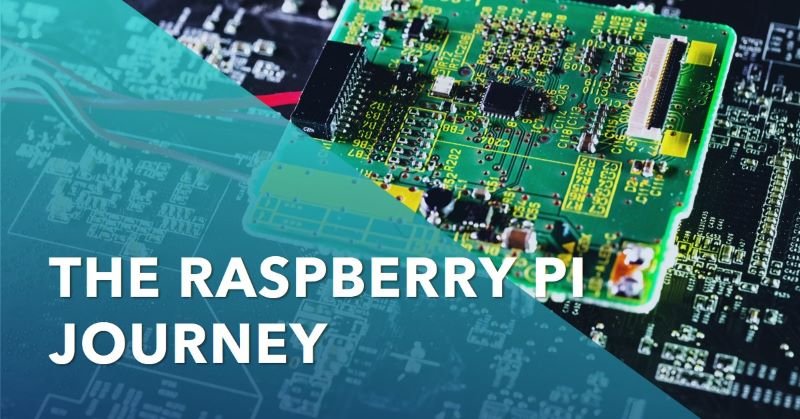
Building a Silicon Design Team: The Raspberry Pi Journey
Over nearly a decade, Raspberry Pi has cultivated a robust ASIC (Application-Specific Integrated Circuit) team based in Cambridge, dedicated to crafting custom silicon chips for their innovative products.
The Genesis of a Silicon Powerhouse
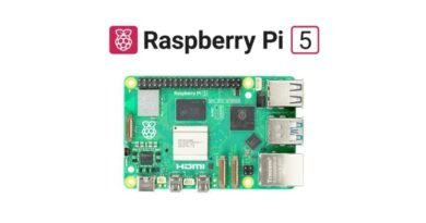
While Raspberry Pi is renowned for its single-board computers and microcontroller boards, it has also made significant strides in silicon design. For the past ten years, Raspberry Pi has been quietly assembling a team of experts to design and produce custom silicon chips. This initiative has led to the creation of key components like the RP2040 microcontroller found in the Raspberry Pi Pico and the RP1 I/O controller used in the latest Raspberry Pi 5.
The Role of Integrated Circuits
Integrated circuits (ICs) are the backbone of modern electronics, performing a multitude of functions across various devices. Made from silicon wafers, these ICs consist of numerous miniaturized and interconnected components. Silicon, being a semiconductor, is ideal for managing electrical currents, which is crucial for the functionality of these circuits.
Inside the ASIC Design Process
Tammy Julyan, ASIC Engineering Director, and Nick Francis, ASIC Technical Director, provided insights into the meticulous process of designing these chips. The journey begins with specifying requirements, which may stem from new ideas, customer needs, or market forecasts. For example, the RP1 chip was designed to handle most of the input and output capabilities for the Raspberry Pi 5, including managing the camera, display, Ethernet, USB, and GPIO.
Designing a new chip involves collaboration across various teams, including software, hardware, and management. The architecture of the chip is refined through iterative discussions, taking into account factors such as performance, power, interfaces, and software requirements.
From Concept to Silicon
Once the architecture is finalized, the design process involves creating and testing the IC layout. This step is crucial to ensure that the chip functions as intended before moving to manufacturing. Verification, a significant part of this process, involves rigorous testing using simulation tools and FPGAs (Field Programmable Gate Arrays) to emulate the hardware in near-real-time.
The HDL (Hardware Description Language) used in chip design, primarily Verilog, is translated into a gate-level netlist that represents the physical layout of the chip. This netlist undergoes a ‘place and route’ process to position the various components and create the intricate connections that form the final chip design.
Manufacturing the Chips
The final design is sent to a wafer foundry for production. The manufacturing process is a complex sequence of steps including photolithography, oxide growth, etching, and ion implantation to create the ICs on silicon wafers. These wafers are then sliced into individual chips, packaged, and tested to ensure they meet quality standards.
A Decade of Innovation
Now, Finally we can say that, Raspberry Pi’s journey from having no ASIC design capability to building a world-class silicon design team is a testament to their commitment to innovation. With a talented team in place, Raspberry Pi continues to push the boundaries of what is possible in custom silicon chip design. We eagerly anticipate the future advancements this team will bring to the world of computing.