Bipolar Junction Transistor (BJT) Explained: Construction, Characteristics and Real World Applications
Bipolar Junction Transistors (BJT) Working and Applications
Bipolar Junction Transistors (BJT) are fundamental components in the field of electronics, playing a critical role in amplification and switching applications. BJTs are three-terminal devices that consist of two pn-junctions, allowing them to control large currents with a small input signal. They are widely used in analog circuits, such as amplifiers, and in digital circuits as switches. The two main types of BJTs, NPN and PNP transistors, differ in their operation and are chosen based on specific application needs. Understanding the construction, symbol, types and working principles of BJTs is essential for leveraging their full potential in electronic design.
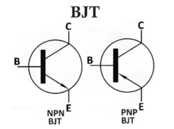
Symbol of BJT
The symbol of a BJT represents its basic structure, which includes three terminals: the emitter (E), the base (B), and the collector (C). The NPN transistor symbol consists of an arrow pointing out from the emitter, indicating the direction of conventional current flow. In contrast, the PNP transistor symbol features an arrow pointing inward towards the emitter. These symbols are crucial in circuit diagrams, helping engineers and technicians quickly identify the type of BJT and its orientation within a circuit.
Types of BJT
BJTs are classified into two main types: NPN and PNP transistors. The primary difference between these types lies in the arrangement and operation of the charge carriers within the transistor. In NPN transistors, electrons are the majority carriers, while in PNP transistors, holes are the majority carriers. Each type has specific applications depending on the required polarity of the voltage and current in the circuit.
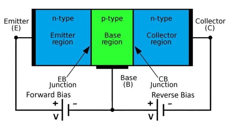
Bipolar Junction Transistors (BJT) Construction
The construction of a BJT involves layering three semiconductor materials with different doping levels. An NPN transistor is constructed with two n-type layers separated by a p-type layer, while a PNP transistor has two p-type layers with an n-type layer in between. These layers form two pn-junctions, with the middle layer, known as the base, being thin and lightly doped. The outer layers, the emitter and the collector, are more heavily doped, with the emitter being the most heavily doped to provide a high injection of charge carriers.
NPN Transistor
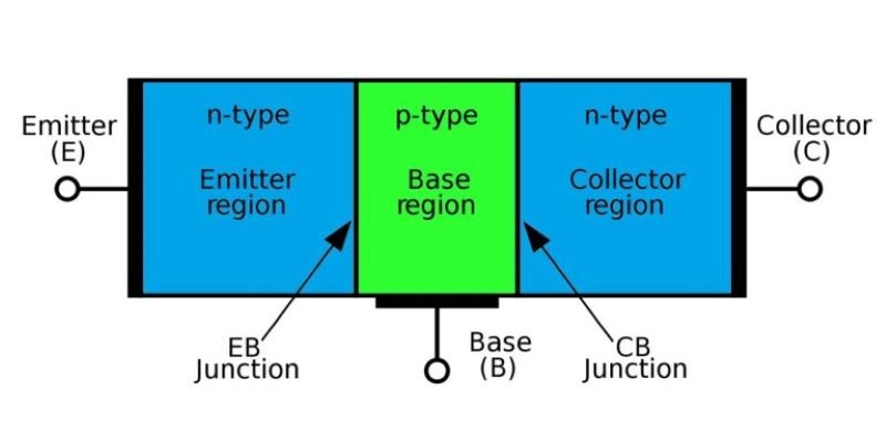
An NPN transistor consists of a thin p-type base sandwiched between two n-type layers, the emitter and the collector. In this configuration, the emitter injects electrons into the base, where they are attracted to the collector due to a positive voltage applied to the collector relative to the emitter. NPN transistors are widely used in amplifying circuits because they provide better electron mobility, resulting in higher efficiency and performance.
PNP Transistor
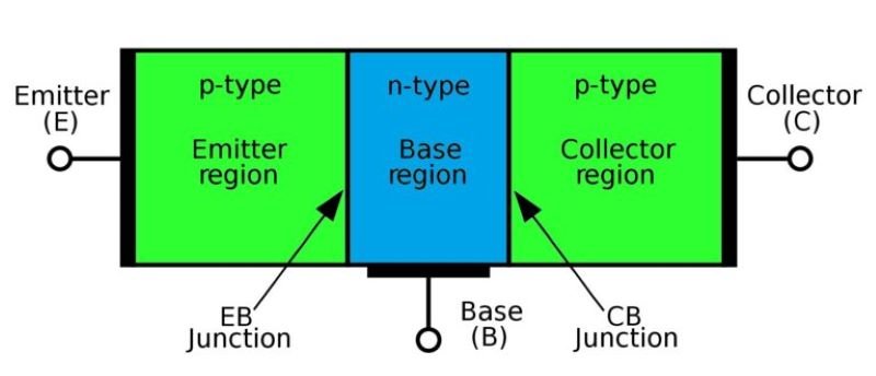
A PNP transistor is constructed with a thin n-type base between two p-type layers, the emitter and the collector. In this type, holes are the majority carriers, and the current flows from the emitter to the collector when the base is negative relative to the emitter. PNP transistors are often used in circuits where a positive voltage is needed for the current to flow. They are less common than NPN transistors but are essential in specific applications that require their unique characteristics.
Physical Structure
The physical structure of a BJT consists of three semiconductor regions: the emitter, base, and collector. The emitter is heavily doped to inject a large number of charge carriers, while the base is lightly doped and very thin to allow most of these carriers to pass through to the collector. The collector, which is moderately doped, collects the carriers from the base. The precise doping levels and thickness of these regions are critical in determining the transistor’s behavior and efficiency in different applications.
Working Principle of BJT
The working principle of a BJT is based on the movement of charge carriers across the two pn-junctions between the emitter, base, and collector. In an NPN transistor, when a small current is applied to the base-emitter junction, it allows a much larger current to flow from the collector to the emitter. This current amplification is due to the injection of electrons from the emitter into the base, where they recombine with holes. The remaining electrons are then swept into the collector, creating the output current. In a PNP transistor, the process is similar but involves holes as the majority carriers. The ability of BJTs to control large currents with small input signals makes them invaluable in amplification and switching circuits.
Biasing of BJT
Biasing a Bipolar Junction Transistor (BJT) is the process of setting its operating point by applying external voltages to its terminals. Proper biasing is crucial for the transistor to function efficiently in amplification or switching applications. There are several methods of biasing a BJT, including fixed bias, emitter bias, and voltage-divider bias. The goal is to ensure that the transistor operates in the desired region, such as the active region for amplification, where the base-emitter junction is forward biased, and the base-collector junction is reverse biased. Proper biasing stabilizes the transistor’s operation, reduces distortion in amplifiers, and ensures consistent performance across varying temperatures and supply voltages.
VI Characteristics of Bipolar Junction Transistors
The VI (Voltage-Current) characteristics of Bipolar Junction Transistors describe how the current flowing through the transistor’s terminals varies with the applied voltage. These characteristics are crucial for understanding the behavior of the transistor in different regions of operation: cutoff, active, and saturation. The curves are plotted for both the base-emitter (input characteristics) and collector-emitter (output characteristics) junctions. The input characteristics represent the base current as a function of the base-emitter voltage, while the output characteristics show the collector current as a function of the collector-emitter voltage for various base currents.
VI Characteristics of NPN BJT
In an NPN transistor, the VI characteristics can be divided into input and output characteristics. The input characteristic curve is obtained by plotting the base current (Ib) against the base-emitter voltage (Vbe) while keeping the collector-emitter voltage (Vce) constant. It shows a typical exponential increase in base current with an increase in Vbe. The output characteristic curve, on the other hand, is obtained by plotting the collector current (Ic) against Vce for various base currents (Ib). It demonstrates that Ic remains constant for a wide range of Vce, indicating that the transistor is in the active region, where it functions as an amplifier.
VI Characteristics of PNP BJT
The VI characteristics of a PNP transistor are similar to those of an NPN transistor, but with polarities reversed. In the input characteristic curve, the base current (Ib) is plotted against the base-emitter voltage (Vbe), with Vce kept constant. However, for a PNP transistor, Vbe is negative, and the base current flows into the base terminal. The output characteristic curve shows the relationship between the collector current (Ic) and the collector-emitter voltage (Vce) for different base currents. In the active region, the collector current is relatively constant, with the base-emitter junction forward biased and the base-collector junction reverse biased.
Advantages and Disadvantages of Bipolar Junction Transistors
Advantages:
- High Gain: BJTs offer a high current gain, making them suitable for amplification purposes.
- Wide Operating Range: BJTs can operate efficiently over a wide range of frequencies, from DC to several MHz.
- Low Output Impedance: BJTs have low output impedance, making them ideal for driving loads.
- Better Noise Performance: In some applications, BJTs exhibit lower noise levels compared to other types of transistors, such as Field Effect Transistors (FETs).
Disadvantages:
- Power Consumption: BJTs consume more power than FETs due to the base current required for operation.
- Thermal Runaway: BJTs are more susceptible to thermal runaway, where an increase in temperature leads to higher current flow, further increasing the temperature.
- Complex Biasing: Proper biasing of BJTs is more complex and requires additional components to stabilize the operating point.
- Limited High-Frequency Response: While BJTs can operate at high frequencies, they are generally outperformed by FETs in RF applications.
Applications of Bipolar Junction Transistors
Bipolar Junction Transistors are used in a wide array of applications, including:
- Amplifiers: BJTs are widely used in audio, radio, and RF amplifiers due to their high gain and linearity.
- Switching Circuits: BJTs function as efficient switches in digital circuits, such as logic gates and microprocessors.
- Oscillators: In oscillator circuits, BJTs help generate stable and precise frequency signals.
- Signal Modulation: BJTs are used in communication systems for amplitude and frequency modulation of signals.
- Voltage Regulation: BJTs are employed in voltage regulator circuits to maintain a constant output voltage.
- Motor Control: In motor drivers, BJTs control the speed and direction of DC motors.
- Temperature Sensors: BJTs can be used in temperature sensing circuits due to their predictable change in current with temperature.
Conclusion
In summary, Bipolar Junction Transistors (BJTs) are indispensable components in modern electronics, offering versatility and reliability in various applications. From amplification and switching to signal modulation and motor control, BJTs serve as the backbone of countless circuits and systems. Understanding their construction, working principles, and VI characteristics is crucial for designing efficient and effective electronic devices. While BJTs offer numerous advantages, such as high gain and low output impedance, they also present challenges like power consumption and thermal management.