How to Design and Optimize PCB Antennas for Better Performance
Printed Circuit Board (PCB) antennas utilize the conductive traces and components on the PCB as their conductors. Due to their compact size, affordability, and straightforward integration into various electronic devices, PCB antennas have become a popular choice. They offer a versatile solution for numerous applications, enhancing the design and functionality of modern electronics. In this blog post we will explore, How to design and optimize PCB Antennas for better Performance!
Designing a PCB Antenna
Let’s see! what are the basic requirements to the designing a PCB Antenna?
Application Requirements
The first step in designing a PCB antenna is understanding the application requirements. This involves determining the type of antenna, frequency range, radiation pattern, gain, and other performance metrics needed for the specific application.
Key Considerations:
- Frequency Range: The application’s frequency range determines the type of antenna. Low-frequency applications might require dipole or loop antennas, while high-frequency applications might need patch antennas.
- Bandwidth: A wider bandwidth allows the antenna to operate over a broader frequency spectrum.
- Gain: Higher gain antennas are necessary for long-distance applications or weak signal environments.
- Polarization: The antenna’s polarization should match the incoming signal’s polarization for optimal efficiency.
- Radiation Pattern: The desired signal directionality affects the choice between omnidirectional and directional antennas.
- Size and Weight: The antenna must fit within the device without adding excessive weight.
- Environmental Factors: Temperature, humidity, and electromagnetic interference (EMI) must be considered during design.
Selecting the Appropriate Type of PCB Antenna
The choice of PCB antenna type is crucial, as it impacts the antenna’s performance characteristics. Here’s an overview of common PCB antennas and their features:
Monopole Antenna
A monopole antenna has a single radiating element and is fed by a coaxial cable. It is omnidirectional and often used in broad coverage applications like wireless communication systems.
Dipole Antenna
A dipole antenna consists of two radiating elements connected by a coaxial cable. It is also omnidirectional and is widely used in FM radio and Wi-Fi networks.
Patch Antenna
A patch antenna has a radiating element placed on a ground plane. It is directional, commonly used in GPS systems and wireless routers.
Loop Antenna
A loop antenna is created by connecting a loop of wire to a power source, usually a coaxial cable. It allows for directional pointing and is used in RFID and AM radio applications.
Yagi Antenna
A Yagi antenna is a directional antenna that focuses radio waves in a specific direction using a dipole and parasitic elements. It is commonly used in radio and television transmission.
Helical Antenna
A helical antenna features a helical-shaped wire, creating a directional antenna. It is used in satellite communication and GPS technology.
Each antenna type has its pros and cons. The selection depends on factors such as frequency range, gain, radiation pattern, and physical dimensions. Sometimes, a combination of antenna types is necessary to achieve the desired performance.
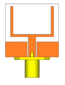
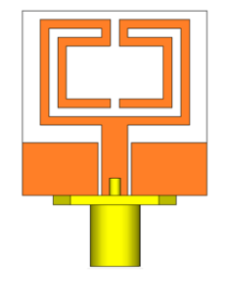
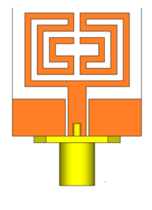
Layout Designing of PCB Antenna
The layout design of a PCB antenna significantly influences its performance. Important factors to consider include the placement of the feed point, ground plane dimensions, and the inclusion of matching networks and filters.
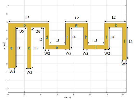
- Feed Point Placement: The location where the signal is introduced into the antenna can affect its efficiency. Proper placement maximizes radiation efficiency.
- Ground Plane: The ground plane shapes the radiation pattern. Adjusting its size and shape can fine-tune the antenna’s performance.
- Matching Networks and Filters: Including these components in the design can enhance the antenna’s functionality and efficiency.
Impedance Matching for PCB Antenna
Impedance matching is crucial for maximizing power transfer and minimizing signal reflections between the antenna and the feeding circuit. Mismatched impedance can reduce antenna efficiency and signal-to-noise ratio.
Methods for Impedance Matching
- Impedance-Matching Network: This network, made of passive components like resistors, capacitors, and inductors, is placed between the feeding circuit and the antenna to adjust impedance.
- Antenna Dimensions: Modifying the physical size of the antenna can tune its impedance to match the feeding circuit. This method can be more complex and time-consuming.
- Simulation Software: Tools like ANSYS HFSS, CST Microwave Studio, and FEKO can simulate the antenna’s performance under various impedance conditions, allowing for pre-fabrication adjustments.
Designing the PCB Antenna Simulation
Simulation tools predict the performance of the antenna before physical fabrication. These tools model the electromagnetic behavior of the antenna and visualize performance metrics like radiation pattern and gain.
Simulation Process:
- 3D Modeling: Create a detailed 3D model of the antenna, including PCB components.
- Electromagnetic Analysis: The software solves electromagnetic equations to predict antenna performance.
- Optimization: Engineers can adjust antenna dimensions or component placements to refine the design through iterative simulations.
- Performance Comparison: The simulated performance is compared to the desired requirements, and adjustments are made until specifications are met.
The Appeal of PCB Antennas
Portability and Compact Design
One of the most significant advantages of PCB antennas is their portability. Designed to occupy minimal space on the PCB, they are ideal for compact devices. By eliminating the need for external antennas, PCB antennas help reduce the overall size and complexity of the device.
Cost-Effectiveness
PCB antennas are cost-effective as they do not require additional components or materials. Fabricating the antenna directly onto the PCB substrate significantly lowers the cost per unit, making PCB antennas an excellent choice for mass production.
Versatility
PCB antennas come in various designs, each with unique benefits and applications. Common types include monopole, dipole, patch, and loop antennas. Selecting the appropriate type involves considering factors such as radiation pattern, gain, and bandwidth, ensuring optimal performance for specific applications.
Adjusting the Radiation Pattern
Fine-tuning the radiation pattern is essential for achieving desired performance. This involves adjusting the antenna’s shape, size, feed point location, and accounting for surrounding objects.
Techniques for Adjusting Radiation Pattern:
- Simulation Software: Simulate the electromagnetic field to predict and adjust the radiation pattern.
- Beamforming: Adjust the phase and amplitude of signals fed to the antenna elements to steer the radiation pattern in a specific direction, creating high-gain, narrow-beam antennas.
Fabrication
Once the design is finalized, the next step is fabricating the antenna. The process includes:
- Substrate Preparation: Clean and surface-treat the PCB substrate for good adhesion.
- Conductor Deposition: Deposit a layer of conductive material, typically copper, onto the substrate.
- Etching: Remove unwanted conductor areas to form the antenna design.
- Resist Removal: Eliminate any remaining resist material.
- Finishing: Apply protective coatings or solder necessary components.
Fabrication quality can impact performance, making precise control over the process crucial.
Advantages of Using a PCB Antenna
Here are some common advantages of using a PCB Antenna!
- Small Size: Custom-designed PCB antennas occupy minimal space, ideal for compact devices.
- Low Cost: Direct fabrication on the PCB substrate reduces costs by eliminating the need for additional components.
- Easy Integration: Integrating PCB antennas into devices is simpler than external antennas, streamlining the design process.
- Customization: Manufacturers can tailor PCB antennas for specific applications and frequency ranges.
- Reliability: PCB antennas are robust against environmental factors like moisture and dust, enhancing reliability.
Conclusion
In conclusion, PCB antennas offer numerous benefits, including compact size, low cost, easy integration, customization, and reliability. As electronic devices become more complex and compact, the demand for efficient and affordable PCB antennas continues to grow. Designing a PCB antenna involves understanding application requirements, selecting the appropriate antenna type, optimizing the layout, ensuring impedance matching, adjusting the radiation pattern, and precise fabrication.
The rising demand for smaller, more sophisticated devices makes PCB antennas an increasingly popular choice for manufacturers. Their cost-effectiveness and ease of integration make them a practical solution for modern electronic products, driving advancements in technology and innovation.