7 Essential Things a PCB Design Engineer Should Know
Printed Circuit Boards (PCBs) are the backbone of modern electronic devices, providing the necessary infrastructure to connect and support electronic components. A PCB design engineer’s role is crucial in ensuring the functionality, reliability, and manufacturability of these boards. Here are seven essential things every good PCB design engineer should master:
1. Basic Electronics
Understanding basic electronics is foundational for any PCB design engineer. This includes knowledge of:
- Electronic Components: Familiarity with resistors, capacitors, inductors, diodes, transistors, and integrated circuits.
- Circuit Theory: Concepts like Ohm’s Law, Kirchhoff’s laws and the behavior of series and parallel circuits.
- Signal Integrity: Awareness of how signals propagate through circuits and the factors that affect them, such as impedance, crosstalk, and noise.
A solid grasp of these fundamentals allows engineers to design circuits that meet functional and performance specifications.
2. Basic Knowledge of PCB
A PCB design engineer must have a thorough understanding of what a PCB is and how it works:
- PCB Materials: Knowledge of different types of PCB materials (e.g., FR-4, Rogers) and their properties.
- Types of PCBs: Single-sided, double-sided and multi-layer PCBs.
- Manufacturing Processes: Awareness of the steps involved in PCB fabrication and assembly, including etching, drilling, plating and soldering.
This knowledge helps in selecting the appropriate materials and processes for a given application.
3. PCB Design Software
Proficiency in PCB design software is essential for creating efficient and manufacturable PCB layouts:
- Popular Tools: Familiarity with tools such as Altium Designer, Eagle, KiCad and OrCAD.
- Schematic Capture: Ability to create and interpret schematic diagrams.
- Layout Design: Skills in placing components, routing traces and defining board outlines.
Being adept in these software tools enables engineers to efficiently design, simulate and verify their PCB designs.
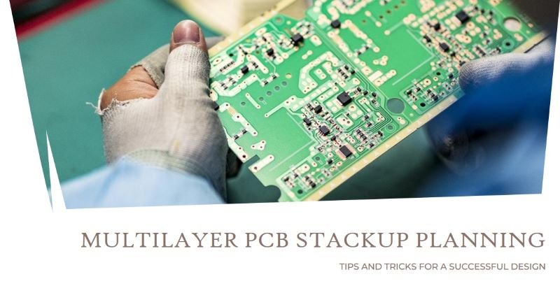
4. PCB Layer Stack-up
Understanding the concept of PCB layer stack-up is crucial for multi-layer PCB design:
- Layer Configuration: Knowledge of how to configure layers for power, ground and signal integrity.
- Impedance Control: Techniques for controlling impedance through appropriate layer stack-up and trace routing.
- Thermal Management: Strategies for managing heat dissipation through layer arrangement and thermal vias.
A well-planned layer stack-up ensures optimal electrical performance and thermal management.
5. PCB Design Rules
Adhering to PCB design rules is essential for ensuring the manufacturability and reliability of the board:
- Design for Manufacturability (DFM): Rules that ensure the design can be manufactured with high yield and low cost.
- Design for Test (DFT): Considerations for making the board easily testable during production.
- Design for Reliability (DFR): Guidelines to ensure the board can operate reliably under expected environmental conditions.
These rules help avoid common design pitfalls and ensure a smooth transition from design to production.
6. 3D Model / Mechanical Design
Integration of mechanical design considerations is important for ensuring that the PCB fits within the intended enclosure and interfaces correctly with other mechanical parts:
- 3D Modeling: Ability to create and work with 3D models of the PCB and its enclosure.
- Mechanical Constraints: Understanding of mechanical constraints such as board thickness, mounting holes, and component height restrictions.
- Thermal and Stress Analysis: Techniques for analyzing and mitigating thermal and mechanical stress on the PCB.
This knowledge ensures that the PCB will not only work electrically but also fit mechanically within its intended application.
7. Detailed Design Review Process
Conducting a thorough design review process is essential for identifying and rectifying potential issues before production:
- Peer Reviews: Engaging in peer reviews to get feedback and catch errors that may have been overlooked.
- Simulation and Testing: Using simulation tools to verify the design and perform tests on prototypes.
- Checklists and Documentation: Utilizing checklists to ensure all design aspects have been considered and maintaining detailed documentation for future reference.
A rigorous design review process helps in catching and correcting issues early, saving time and cost in the long run.
Conclusion
In conclusion, A good PCB design engineer combines knowledge of basic electronics, PCB fundamentals, design software proficiency, layer stack-up expertise, adherence to design rules, mechanical design integration, and a thorough design review process. Mastery of these areas ensures the creation of PCBs that are not only functional and reliable but also manufacturable and cost-effective. As technology continues to evolve, staying updated with the latest advancements and best practices in PCB design is crucial for success in this field.