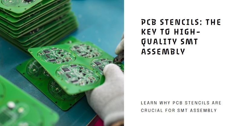
Why PCB Stencil Are Key to High-Quality SMT Assembly?
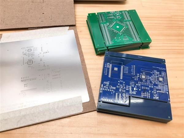
A PCB (Printed Circuit Board) stencil is an essential element in Surface Mount Technology (SMT) assembly. It is crucial for ensuring the precision and uniformity of SMT assembly outcomes, which directly impact the functionality and performance of the final product. Also known as an SMT stencil or Circuit Board stencil, the PCB stencil is used to apply solder paste to the PCB. This paste is then utilized to attach SMT components to the board.
Without a PCB stencil, achieving high-quality SMT assembly results is difficult, and the likelihood of defects and errors increases substantially. The significance of the PCB stencil cannot be overstated, as it helps regulate the amount of solder paste applied, ensures accurate application, and prevents common defects like bridging and tombstoning.
What is a PCB Stencil?
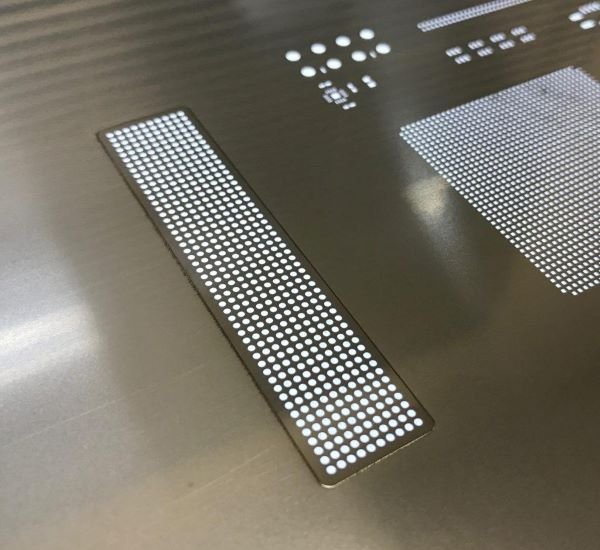
A Printed Circuit Board (PCB) stencil is an indispensable tool in the realm of surface mount technology (SMT). These stencils are precisely engineered to facilitate the accurate application of solder paste to the PCB. The primary function of a PCB stencil is to ensure that the solder paste is deposited onto the board in an exact manner, aligning perfectly with the pads on the PCB where the components will be placed. This precision is achieved through meticulously designed apertures in the stencil, which correspond to the layout of the pads.
The use of PCB stencils in electronics manufacturing offers several significant benefits. Firstly, it enhances the consistency and uniformity of solder paste application, which is crucial for the reliable functioning of the electronic components. Inconsistent solder paste application can lead to issues such as solder bridges, insufficient solder joints, or component misalignment, all of which can compromise the performance and durability of the electronic device.
Types of PCB Stencils
The three primary types of PCB stencils are framed stencils, step stencils, and frameless stencils, each catering to particular needs within the production environment.
Framed Stencil
Framed stencils, also known as mesh-mounted stencils, are mounted on a frame that provides high stability and ease of use. These stencils are ideal for high-volume production runs due to their robustness and the ability to maintain consistent tension. This stability ensures precise and repeatable solder paste application, which is crucial for mass production. However, framed stencils can be more expensive and take up more storage space compared to their frameless counterparts. Nonetheless, their durability and reliability make them a preferred choice for large-scale manufacturing processes.
Step Stencil
Step stencils are designed with varying thicknesses in different areas, allowing for precise control over solder paste deposition. This feature is particularly beneficial for complex PCBs that include components of various sizes and shapes. By adjusting the stencil thickness, manufacturers can ensure optimal solder paste volume for each component, reducing the risk of defects such as solder bridging or insufficient solder. Step stencils require meticulous design and fabrication, making them more expensive than standard stencils. Despite this, their ability to handle intricate board designs makes them indispensable in advanced electronics manufacturing.
Frameless Stencil
Frameless stencils are a flexible and cost-effective option, suitable for both prototype and low-volume production. These stencils are not permanently mounted on a frame; instead, they require a separate frame system for tensioning during use. This modularity allows for easy storage and reduced costs, as multiple stencils can share a single frame system. While frameless stencils may lack the immediate stability of framed versions, they offer significant advantages in terms of versatility and cost savings, particularly for small-scale or experimental projects.
How to Choose the Right PCB Stencil
Choosing the right PCB stencil is crucial for achieving efficient and accurate solder paste application, significantly impacting the quality and reliability of the final product. Several key factors should be considered to ensure the selected stencil meets the specific needs of your production environment.
Production Volume: The volume of production plays a significant role in stencil selection. For high-volume production environments, framed stencils are often more advantageous. These stencils are more durable and provide consistent results over prolonged use. Conversely, for low-volume production or prototyping, frameless stencils might be more suitable. Frameless stencils are cost-effective and offer flexibility, making them ideal for projects where stencil changes are frequent, or production runs are shorter.
Board Complexity: The complexity of the PCB design is another critical consideration. Boards with a mix of large and small components or intricate layouts may benefit from step stencils. Step stencils have varying thicknesses, allowing precise control over solder paste deposition. This ensures that each component receives the appropriate amount of solder paste, improving the overall assembly quality and reliability.
Budget Constraints: Budget is always a concern in manufacturing. While framed stencils may have a higher initial cost, their durability can lead to cost savings over time due to reduced replacement frequency. Frameless stencils, although cheaper initially, might incur higher costs in the long run if they need frequent replacement. Balancing the initial investment with long-term cost-effectiveness is essential for making an informed decision.
Precision Requirements: The precision of the stencil apertures directly affects the reliability of solder joints. High-quality stencils with precise apertures ensure accurate solder paste deposition, reducing the risk of defects such as bridging or insufficient solder. Investing in a high-precision stencil can significantly improve the manufacturing yield and the long-term reliability of the assembled PCBs.
PCB Stencil Framework
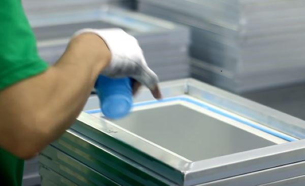
The framework of a PCB stencil is crucial when choosing a stencil for a specific application. It provides support, keeping the stencil flat and in position during the printing process. This framework significantly impacts the stencil’s accuracy, consistency, durability, cost, and ease of use. In this section, we will examine the various materials used for PCB stencil frameworks, their benefits and drawbacks, and the key factors to consider when selecting a framework material.
Materials Used for PCB Stencil Framework
The most common materials for PCB stencil frameworks include stainless steel, nickel, and aluminum.
- Stainless Steel: Stainless steel is the most frequently used material for PCB stencil frameworks. It is strong, durable, and resistant to corrosion and wear. Its easy maintenance makes it suitable for high-volume production runs. However, stainless steel is relatively heavy, which can complicate handling and transportation. Additionally, it is more expensive than other materials.
- Nickel: Nickel is less commonly used but offers several advantages. It is lighter and more flexible than stainless steel, making it easier to handle and transport. Nickel is also highly resistant to corrosion and wear, making it ideal for harsh environments. However, it is more expensive than stainless steel and can be more challenging to clean and maintain.
- Aluminum: Aluminum is a lightweight and cost-effective option for PCB stencil frameworks. It is easy to handle and transport and can be machined or formed to meet specific requirements. However, aluminum is less durable than stainless steel or nickel and is more susceptible to wear and corrosion. It is best suited for low- to medium-volume production runs.
Factors to Consider When Selecting Framework Material
When choosing the framework material for a PCB stencil, consider the following factors:
- Size and complexity of the PCB
- Type of components used
- Required accuracy and consistency of the solder paste application
- Cost and budget constraints
- Handling and transportation needs
- Environmental factors such as temperature and humidity
Polishing Process for PCB Stencil
Various methods are used for polishing PCB stencils, including:
- Mechanical Polishing: This involves using a mechanical tool, like a polishing pad or brush, to remove burrs or scratches from the stencil material. It is a simple and cost-effective method but can be time-consuming and may not provide the same precision as other methods.
- Chemical Polishing: This method uses a chemical solution to dissolve imperfections on the stencil material. It is highly precise and can produce a smooth, consistent surface finish but requires careful handling and can be expensive.
- Electropolishing: This involves using an electric current to dissolve imperfections on the stencil material. It is highly precise and produces a smooth, consistent surface finish but requires specialized equipment and can be expensive.
Factors to Consider When Selecting Polishing Method
When choosing a polishing method for PCB stencils, consider the following factors:
- Compatibility with the stencil material
- Required precision and consistency
- Budget constraints
- Time constraints
Optimizing Stencil Size
The size optimization of a PCB stencil is important when designing a stencil for a particular application. The stencil size affects the amount of solder paste applied, the accuracy and consistency of the paste application, and the overall cost and efficiency of the manufacturing process.
Factors to Consider When Optimizing Stencil Size
Consider the following when optimizing the size of a PCB stencil:
- The dimensions of the PCB, allowing a small margin around the edges for alignment and handling.
- The size and shape of the components used, with a small margin around them for alignment and paste application.
- The printing method (manual or automated) to ensure consistent and accurate paste application.
- The desired paste volume, based on the type and size of components and the required solder joint reliability.
- Compatibility with the manufacturing process, including handling, cleaning, and storage requirements.
Summary
In summary, PCB stencils are essential for achieving high-quality SMT assembly. They enable accurate and consistent application of solder paste to the PCB, which is crucial for reliable and robust solder joints. Careful consideration of the framework, polishing method, and size optimization of the stencil is necessary to ensure optimal performance and high-quality results.