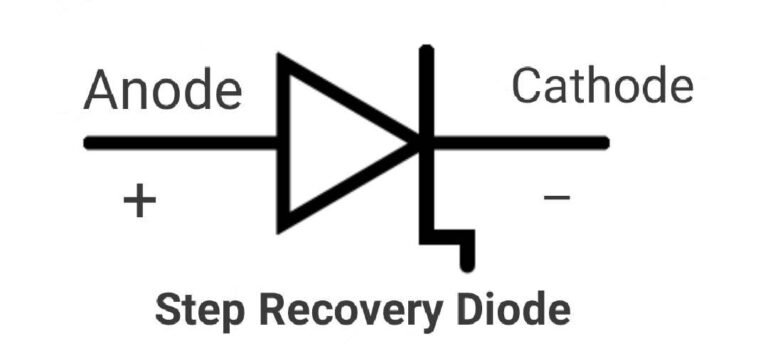
Step Recovery Diode Symbol, Construction, Working & Applications
Introduction to Step Recovery Diode (SRD)
The Step Recovery Diode (SRD) is a specialized semiconductor device known for its ability to generate sharp pulses and operate at high frequencies. Unlike regular diodes, SRDs are designed to take advantage of the charge storage and rapid depletion characteristics at the P-N junction, making them indispensable in applications such as frequency multipliers, pulse generators, and microwave circuits.
With a unique construction and doping profile, SRDs are capable of switching from conducting to non-conducting states almost instantaneously, which is why they are widely used in high-speed and high-frequency electronic systems.
Working Principle of SRD
The Step Recovery Diode (SRD) operates based on the principle of charge storage and rapid depletion. When the diode is forward biased, it accumulates charge within its junction. As the bias is reversed, the stored charge is rapidly released, leading to a sharp change in current. This sudden current transition is utilized in high-frequency pulse generation and waveform shaping applications, making SRDs ideal for use in frequency multipliers, pulse generators, and harmonic generation circuits.
Construction of Step Recovery Diode
The construction of a Step Recovery Diode involves carefully designing the semiconductor layers and doping profiles to achieve the desired charge storage and release characteristics. The diode consists of a P-N junction with specialized doping levels and materials to ensure efficient charge accumulation and rapid depletion. The junction is formed with precise control over the thickness and doping concentration of each layer, optimizing the diode’s performance in high-speed switching applications.
Materials and Doping
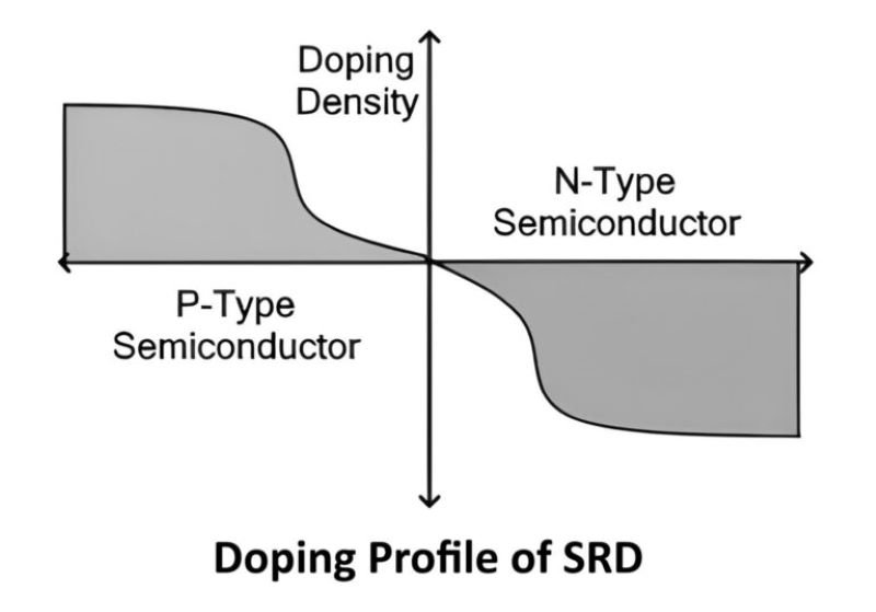
The materials and doping profiles of an SRD are crucial in determining its performance. Typically, silicon is used as the semiconductor material due to its well-understood properties and compatibility with existing semiconductor fabrication processes. The doping process is carefully controlled to create regions with varying levels of impurities, which affect the diode’s charge storage capacity and switching speed.
Semiconductor Material
Silicon is commonly used as the semiconductor material for SRDs due to its excellent electrical properties, availability, and ease of integration into existing manufacturing processes. The choice of silicon ensures that the diode can handle high voltages and frequencies, making it suitable for a wide range of applications.
Doping Profile
The doping profile of an SRD is designed to create regions with different levels of charge carriers (electrons and holes). The P-type region is doped with acceptor impurities, while the N-type region is doped with donor impurities. The precise control of doping concentrations allows the diode to accumulate and release charge efficiently, enabling fast switching times.
Layer Structure
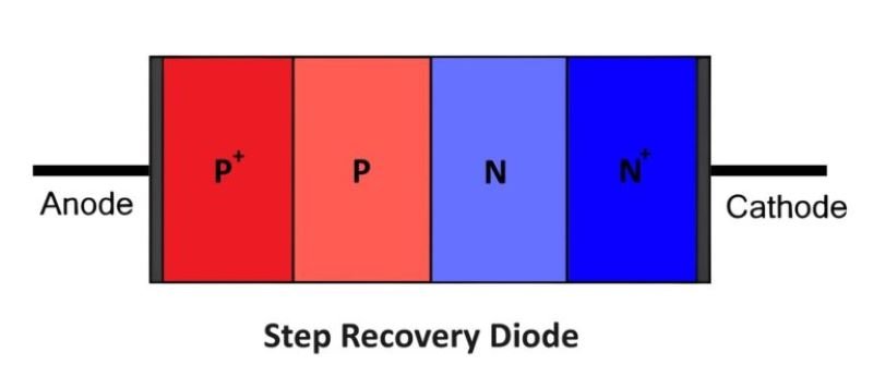
The SRD consists of multiple layers, each with a specific function. The P-type and N-type regions form the core of the diode, where the charge accumulation and release occur. Additional layers, such as heavily doped N+ and P+ regions, may be included to enhance the diode’s electrical characteristics and improve its performance in high-frequency applications.
Construction Steps
- Wafer Preparation: The process begins with the preparation of a silicon wafer, which serves as the base material for the diode.
- Doping: Controlled doping is performed to create the P-type and N-type regions, forming the P-N junction.
- Layer Deposition: Additional layers, such as the heavily doped regions, are deposited onto the wafer to optimize the diode’s performance.
- Junction Formation: The P-N junction is carefully formed, ensuring that the diode has the desired charge storage and release properties.
- Final Processing: The wafer undergoes further processing steps, including etching, metallization, and packaging, to create the final SRD device.
Structural Diagram
The structural diagram of an SRD typically includes a cross-sectional view of the P-N junction, highlighting the P-type and N-type regions, doping concentrations, and additional layers. This diagram is essential for understanding how the diode’s construction influences its performance in high-speed applications.
VI Characteristics of Step Recovery Diode (SRD)
The VI characteristics of an SRD are crucial in understanding its behavior under different biasing conditions. The diode exhibits unique characteristics in both the forward and reverse bias regions, which are exploited in various applications.
Region of Forward Bias
In the forward bias region, the SRD allows current to flow through the P-N junction, leading to the accumulation of charge. The voltage across the diode increases gradually as the current increases, resulting in a relatively linear VI curve. This region is characterized by low resistance and high charge storage.
Region of Reverse Bias
When the diode is reverse biased, the accumulated charge is rapidly depleted, leading to a sudden drop in current. The reverse bias region is characterized by a steep VI curve, indicating the diode’s ability to switch quickly from conducting to non-conducting states. This property is essential for applications requiring sharp pulse generation and high-frequency operation.
Key VI Characteristics
- High Reverse Recovery Time: The time it takes for the diode to switch from conducting to non-conducting states is critical in high-speed applications.
- Steep Reverse Bias Region: The sharp transition in the reverse bias region is a key characteristic of SRDs.
- Low Forward Voltage Drop: The diode exhibits a low voltage drop in the forward bias region, ensuring efficient operation.
VI Curve Illustration
The VI curve of an SRD can be illustrated with a graph showing the current (I) on the y-axis and the voltage (V) on the x-axis. The curve will depict a linear rise in the forward bias region, followed by a steep drop in the reverse bias region, highlighting the diode’s fast switching capabilities.
Advantages of Step Recovery Diode (SRD)
- High-Speed Operation: SRDs are capable of extremely fast switching due to their ability to quickly deplete stored charge, making them ideal for high-frequency applications.
- Sharp Pulse Generation: The sudden change in current during reverse recovery allows SRDs to generate sharp pulses, which are crucial in pulse shaping and frequency multiplication.
- Efficiency in Frequency Multiplication: SRDs are highly efficient in generating harmonics, making them effective in frequency multipliers where multiple higher frequency signals are derived from a single input signal.
- Low Forward Voltage Drop: SRDs exhibit a low forward voltage drop, which minimizes power loss during operation, contributing to the overall efficiency of the circuit.
- Reliability: With robust construction and precise doping, SRDs offer reliable performance in demanding environments, ensuring consistent operation in high-speed circuits.
Disadvantages of Step Recovery Diode (SRD)
- Complex Manufacturing Process: The precise doping and layer structure required for SRDs make their manufacturing process complex and costly compared to standard diodes.
- Limited Power Handling: SRDs are typically designed for low-power applications, which limits their use in circuits requiring high power handling capabilities.
- Sensitivity to Temperature: SRDs can be sensitive to temperature variations, which may affect their performance in certain environments, requiring additional thermal management solutions.
- Narrow Application Range: The specialized nature of SRDs means they are not as versatile as other diodes, limiting their use to specific high-frequency and pulse generation applications.
Applications of Step Recovery Diode
- Frequency Multipliers: SRDs are widely used in frequency multiplier circuits, where they generate higher harmonics of the input signal, essential in communication systems and radar technology.
- Pulse Generators: The sharp pulse generation capability of SRDs makes them ideal for use in pulse generators, which are critical in various timing and control applications.
- Microwave Circuits: SRDs are employed in microwave circuits for their ability to operate at high frequencies, making them suitable for use in RF and microwave communication systems.
- Waveform Shaping: In applications where precise waveform shaping is required, SRDs play a crucial role by generating the necessary sharp transitions in signal waveforms.
- Mixers and Demodulators: SRDs are used in mixers and demodulators in communication systems, where their fast switching speeds and sharp pulse generation improve signal processing performance.
Conclusion
In conclusion, The Step Recovery Diode (SRD) is a highly specialized component that excels in high-frequency and pulse generation applications. Its ability to quickly switch states and generate sharp pulses makes it invaluable in communication systems, microwave circuits, and frequency multipliers. However, the complexity of its manufacturing process and its limited power handling capabilities are factors to consider when choosing an SRD for specific applications. Despite these limitations, SRDs remain a critical component in many high-speed electronic systems, providing reliable and efficient performance where precise timing and high frequencies are essential.