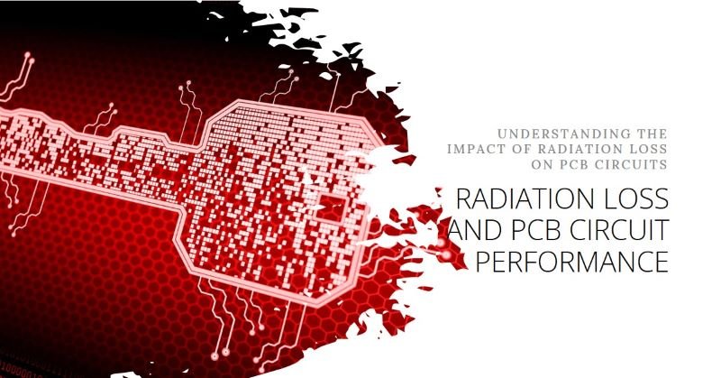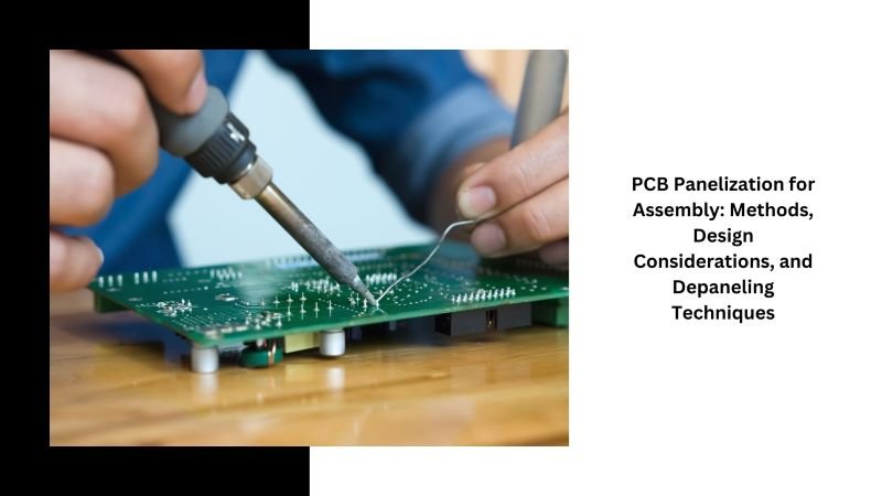
PCB Panelization for Assembly: Methods, Design Considerations, and Depaneling Techniques
Printed Circuit Board (PCB) panelization is a manufacturing technique that combines multiple PCBs into a single, larger panel. This method enhances production efficiency, reduces costs, and simplifies handling during assembly processes. By treating several smaller boards as one unit, manufacturers can streamline operations, optimize resource utilization, and ensure consistent quality across batches.
Understanding PCB Panelization
Panelization involves arranging multiple PCB designs onto a larger board, known as a panel or array. This approach allows for simultaneous processing of multiple boards, leading to increased throughput and reduced production time. After assembly and testing, individual PCBs are separated from the panel through a process called depaneling.
PCB panelization significantly enhances the efficiency of the overall PCB assembly process. By grouping multiple boards, manufacturers can optimize assembly time and reduce handling errors
Benefits of PCB Panelization
- Enhanced Production Efficiency: Processing multiple boards simultaneously reduces the number of production cycles, leading to faster turnaround times.
- Cost Reduction: Combining boards minimizes material wastage and optimizes the use of manufacturing resources, resulting in cost savings.
- Simplified Handling: Larger panels are easier to handle during assembly, reducing the risk of damage to individual boards and improving overall yield.
- Improved Quality Control: Uniform processing conditions across all boards in a panel ensure consistent quality and facilitate easier defect detection.
Panelization Methods
Several techniques are employed to panelize PCBs, each with its advantages and considerations:
1. V-Scoring (V-Cut, V-Groove)
V-scoring involves making V-shaped grooves on both sides of the PCB panel, creating a partial cut that allows for easy separation of individual boards. This method is suitable for rectangular or square boards without overhanging components.
- Spacing: Boards can be placed with a spacing of either 0mm or 3mm between them.
- Considerations: V-scoring must be continuous across the panel and cannot be stopped midway. For panels with multiple different board designs, it’s advisable to use tab routing instead of V-scoring to accommodate varying shapes and sizes.
2. Tab Routing (Tab Breakout, Breakaway Tabs)
Tab routing uses perforated tabs or solid tabs to connect individual boards within a panel. These tabs are broken or cut during depaneling.
- Types:
- With Breaking Holes (Stamp Holes): Perforated holes are added to the tabs to facilitate easier breaking.
- Hole Diameter: ≥0.45mm, typically between 0.55mm-0.6mm.
- Hole Spacing: ≥0.35mm.
- Number of Holes per Tab: Typically 5-6 holes to balance strength and ease of separation.
- Without Holes: Solid tabs without perforations.
- Tab Width: At least 2mm.
- With Breaking Holes (Stamp Holes): Perforated holes are added to the tabs to facilitate easier breaking.
- Spacing: A 1.6mm gap is required between boards to accommodate the routing path.
3. Combination of V-Scoring and Tab Routing
In some cases, a combination of both methods is used to optimize panel strength and ease of depaneling.
- Spacing:
- V-Scoring Area: 3mm spacing.
- Tab Routing Area: 1.6mm spacing.
Design Considerations for Panelization
Effective panelization requires careful planning to ensure compatibility with assembly processes and equipment. Key considerations include:
- Panel Size and Thickness
- Standard Sizes: Common panel sizes range from 50x50mm to 330x530mm, depending on manufacturing capabilities and equipment constraints.
- Thickness: Typically ranges from 0.8mm to 2.4mm, depending on the application’s mechanical requirements and assembly process.
- Fiducial Marks
Fiducial marks are reference points used by automated assembly equipment to ensure accurate component placement.
- Quantity: Typically, three fiducial marks are added to each panel.
- Dimensions: Each mark has a 1.0mm diameter with a 1.7mm solder mask opening.
- Placement: Located in the middle of the edge rails to provide consistent reference points across the panel.
- Mounting Holes
Mounting holes are used to secure the panel during assembly and testing.
- Quantity: Typically, four mounting holes are added per panel.
- Dimensions and Location: Determined based on equipment requirements and panel design, ensuring compatibility with assembly fixtures.
- Component Placement Near Edges
Components placed too close to the edges can be damaged during depaneling. It’s advisable to maintain a safe distance between components and the panel edge to prevent mechanical stress and potential damage.
- Tooling Strips and Rails
Adding tooling strips or rails around the panel’s perimeter provides additional support and facilitates handling during assembly. These strips can include tooling holes, fiducial marks, and test coupons, enhancing the overall assembly process.
Depaneling Methods
After assembly and testing, individual PCBs must be separated from the panel. The choice of depaneling method depends on the panelization technique used and the specific requirements of the boards. Common depaneling methods include:
- Manual Breaking Used primarily for V-scored panels, where the boards are snapped apart by applying pressure along the scored lines. This method is simple but may introduce mechanical stress, potentially damaging sensitive components.
- Router Cutting CNC routers equipped with high-speed rotating blades cut along the routed paths, providing precise separation without excessive mechanical stress.
- Laser Cutting Laser cutting offers high precision and is suitable for complex board geometries but is generally slower and more expensive than other methods.
- Die Cutting Suitable for high-volume production, die cutting uses custom-shaped dies to punch out individual boards from the panel.
Conclusion
In conclusion, PCB panelization is a critical process in modern electronics manufacturing, offering numerous benefits in terms of efficiency, cost reduction, and quality control. Selecting the appropriate panelization method and design considerations ensures that the final product meets the desired performance and reliability standards. By understanding the various techniques and best practices associated with PCB panelization, manufacturers can optimize their production processes and deliver high-quality products to market more efficiently.