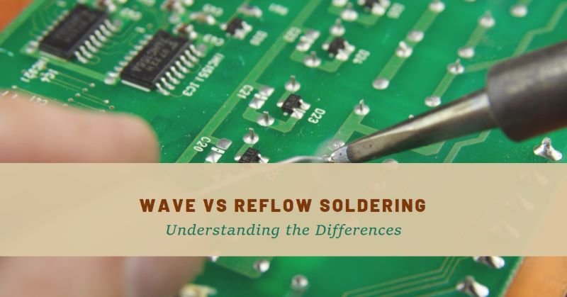
Difference b/w Wave Soldering and Reflow Soldering in PCB Assembly
A critical step in PCB assembly is soldering, which involves the use of molten solder to affix components onto the board. Soldering not only secures the components but also establishes electrical connections between them, ensuring the seamless flow of electrical signals. Without effective soldering, the integrity of the electronic device could be compromised, leading to potential failures and malfunctions.
There are two primary soldering techniques used in PCB assembly: reflow soldering and wave soldering. Reflow soldering is typically employed for Surface Mount Technology (SMT) components, where solder paste is applied to the PCB pads, components are placed, and the assembly is heated to melt the solder and create strong joints. Conversely, wave soldering is used mainly for Through-Hole Technology (THT) components. In this method, the PCB is passed over a wave of molten solder, which attaches the components to the board.
Understanding Reflow Soldering
Reflow soldering is a critical process in Surface Mount Technology (SMT) for assembling printed circuit boards (PCBs). This method involves several steps, starting with the precise application of solder paste onto the PCB pads. The solder paste, a mixture of powdered solder and flux, is carefully deposited using a stencil to ensure accuracy and consistency.
Once the solder paste is applied, SMT components are placed onto the PCB. This step often employs automated pick-and-place machines, which enhance placement accuracy and speed, particularly beneficial for densely packed and complex PCB designs. The components adhere to the solder paste, which temporarily holds them in place until the soldering process is completed.
The next phase involves passing the PCB assembly through a reflow oven. The reflow oven operates on a meticulously controlled temperature profile divided into four main stages: preheating, soaking, reflow, and cooling. In the preheating stage, the temperature gradually rises to activate the flux in the solder paste, which helps remove oxides and promotes wetting. The soaking stage then maintains a stable temperature to ensure uniform heating across the PCB.
During the reflow stage, the temperature peaks, causing the solder particles in the paste to melt and form robust electrical connections between the components and the PCB. Finally, the cooling stage allows the solder to solidify, creating strong, reliable joints.
Advantages of Reflow Soldering
Reflow soldering offers several advantages, including high precision and the ability to handle complex, densely populated PCBs. The process is highly compatible with automation, thus enhancing efficiency and consistency in mass production.
Challenges in Reflow Soldering
However, it comes with its challenges, such as potential solder paste defects like voids or insufficient coverage. Additionally, thermal stress during the reflow process can affect sensitive components, necessitating careful temperature control to mitigate any adverse effects.
Understanding Wave Soldering
Wave soldering is a critical process in printed circuit board (PCB) assembly, particularly effective for Through-Hole Technology (THT) components. This technique involves several stages to ensure robust and reliable electrical connections. The wave soldering process begins with the application of flux. The flux is essential for cleaning and preparing the component leads and the PCB surface by removing oxides and contaminants. This cleaning action ensures that the solder can form strong, reliable joints.
Following the flux application, the PCB undergoes a preheating phase. Preheating serves a dual purpose: it activates the flux and helps to prevent thermal shock by gradually increasing the temperature of the PCB. This step is crucial because sudden temperature changes can damage both the PCB and its components.
The core of the wave soldering process is the passage of the PCB over a wave of molten solder. During this stage, the PCB is conveyed over a wave of liquid solder, which makes contact with the exposed leads and pads, creating electrical connections. This method is particularly advantageous for THT components as it ensures that solder fills the plated through-holes, establishing strong mechanical and electrical bonds.
Advantages of Wave Soldering
Advantages of wave soldering is its speed and efficiency. It allows for the soldering of multiple components simultaneously and in some cases both sides of the PCB can be soldered in a single pass. This capability significantly enhances productivity in high-volume manufacturing environments.
Challenges in Wave Soldering
However, wave soldering is not without its challenges. Solder bridging, where excess solder creates unintended connections between adjacent leads is a common issue. Additionally, the process parameters, such as the temperature and speed of the solder wave, require precise control to avoid thermal damage to components and ensure quality solder joints. Proper maintenance and calibration of the wave soldering equipment are essential to mitigate these risks and achieve consistent results.
Comparative Analysis and Applications in Industry
Reflow soldering and wave soldering are two predominant methods used in printed circuit board (PCB) assembly, each with distinct advantages tailored to specific applications. Reflow soldering is predominantly used for Surface-Mount Technology (SMT) components. This method involves applying solder paste to the PCB, placing the SMT components, and then heating the assembly to melt the solder, forming electrical connections. It is particularly advantageous for high-density, complex PCB designs with numerous small components, such as those found in consumer electronics like smartphones and laptops.
Wave soldering, on the other hand, is primarily employed for Through-Hole Technology (THT) components. In this process, the PCB is passed over a wave of molten solder, which adheres to the exposed metal areas, forming solid electrical connections. This method is highly efficient for large-scale production runs and is well-suited for simpler PCB designs or situations where mechanical strength is critical, such as in automotive and industrial equipment applications.
When considering production volume, reflow soldering is often preferred for medium to high-volume manufacturing due to its precision and efficiency in handling small, intricate components. Wave soldering, however, remains the method of choice for high-volume assemblies involving THT components, where speed and cost-effectiveness are paramount. In scenarios involving mixed technology assemblies (both SMT and THT components), a combination of reflow and wave soldering may be employed to capitalize on the strengths of each method.
Industry applications for each method vary significantly. Reflow soldering is extensively used in the consumer electronics sector, where miniaturization and complexity are key drivers. Wave soldering finds its niche in the automotive industry, where reliability and durability are crucial. Industrial equipment, which often involves robust and sizable components, also benefits from the wave soldering process.
Future Aspects
Looking ahead, advancements in PCB soldering technology are poised to reshape the industry. Hybrid soldering techniques, which integrate both reflow and wave soldering processes, are gaining traction for their versatility. Emerging technologies like 3D printing and artificial intelligence (AI) are also set to revolutionize PCB assembly, offering unprecedented precision and efficiency. These innovations promise to enhance the capabilities of both reflow and wave soldering, catering to the evolving demands of modern electronics manufacturing.