Understanding the 741 OP AMP: Pin Configuration, Circuit Diagram and Working
Operational amplifiers, commonly referred to as OP AMPs, are versatile and widely used electronic components in analog circuits. They serve as the building blocks for a variety of applications, such as signal amplification, filtering, and mathematical operations like addition, subtraction, integration, and differentiation. Among the various OP AMPs available, the 741 OP AMP has gained iconic status due to its simplicity, reliability, and wide applicability.
The 741 OP AMP is a general-purpose operational amplifier that features high gain, internal frequency compensation, and a standard 8-pin Dual In-line Package (DIP) configuration. It is highly regarded in the field of electronics for its ease of use and is an excellent choice for learners and professionals alike. In this article, we will explore the specifications, pin configuration, and working principles of the 741 OP AMP, along with its circuit diagram.
Specifications and Pin Configuration
Detailed Specifications of the 741 OP AMP:
- Input Offset Voltage: Typically 2 mV to 6 mV.
- Input Impedance: High, typically 2 MΩ.
- Output Impedance: Low, around 75 Ω.
- Gain Bandwidth Product: Approximately 1 MHz.
- Slew Rate: 0.5 V/μs.
- Maximum Supply Voltage: ±15V (or 30V total).
- Typical Voltage Gain: 200,000 (open loop).
- Common-Mode Rejection Ratio (CMRR): 70 dB.
- Package Type: Standard 8-pin DIP or other configurations like SOIC.
- Operating Temperature Range: 0°C to 70°C (commercial grade).
Explanation of the Pin Configuration (8-pin DIP Layout)
The 741 OP AMP comes in a standard 8-pin DIP package, with each pin serving a specific function:
- Pin 1 (Offset Null): Used to eliminate offset voltage by connecting to an external potentiometer.
- Pin 2 (Inverting Input): The input where the signal is applied for inversion.
- Pin 3 (Non-Inverting Input): The input where the signal is applied for non-inversion.
- Pin 4 (V-): The negative power supply terminal (often connected to -Vcc).
- Pin 5 (Offset Null): Same function as Pin 1 for offset adjustment.
- Pin 6 (Output): The output terminal of the amplifier.
- Pin 7 (V+): The positive power supply terminal (often connected to +Vcc).
- Pin 8 (No Connection): Generally not connected internally, can be left unused.
Function of Each Pin
- Offset Null (Pins 1 and 5): Allows fine-tuning of the output to eliminate offset voltage.
- Inverting Input (Pin 2): Provides a 180-degree phase shift to the input signal.
- Non-Inverting Input (Pin 3): Amplifies the signal without phase inversion.
- Power Supply (Pins 4 and 7): Provides the required voltage for the OP AMP to function.
- Output (Pin 6): Delivers the amplified signal.
- No Connection (Pin 8): Reserved and typically unused.
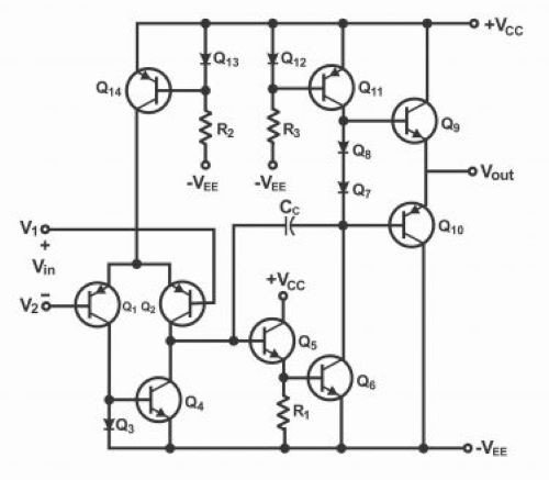
Circuit Diagram of the 741 OP AMP
To demonstrate the functionality of the 741 OP AMP, we will consider a simple non-inverting amplifier circuit. This configuration is commonly used to amplify signals while maintaining their original phase.
Schematic Representation of the Circuit Diagram

The basic non-inverting amplifier circuit includes the following components:
- A 741 OP AMP.
- Resistors (R1 and R2) to set the gain.
- A power supply (±15V).
- Input and output connections for the signal.
Description of the Components Used and Their Connections
- 741 OP AMP: The main component that amplifies the input signal.
- Resistors R1 and R2: These resistors form a voltage divider network to set the gain of the amplifier. The gain is determined by the formula:
Gain (A) = 1 + (R2 / R1)
- Power Supply: Provides the necessary voltage for the OP AMP to operate, typically ±15V.
- Input Signal: The signal to be amplified is fed into the non-inverting input (Pin 3).
- Output Signal: The amplified signal is obtained from the output terminal (Pin 6).
Working of the 741 OP AMP Circuit
Step-by-Step Explanation of the Circuit’s Operation
- The input signal is applied to the non-inverting input (Pin 3) of the OP AMP.
- The inverting input (Pin 2) is connected to a voltage divider network formed by R1 and R2, creating a feedback loop.
- The OP AMP amplifies the difference between the voltages at the inverting and non-inverting inputs.
- The gain of the circuit is determined by the values of R1 and R2, according to the formula:
Gain (A) = 1 + (R2 / R1)
- The amplified signal is delivered at the output terminal (Pin 6).
- Feedback ensures stability and minimizes distortion, maintaining a linear relationship between input and output.
How the Input Signal is Processed
- The input signal is amplified without inversion, preserving the phase.
- The feedback loop stabilizes the gain and controls the output voltage swing to stay within the supply limits.
Key Concepts
- Gain: Determines how much the input signal is amplified.
- Feedback: A portion of the output is fed back to the input to stabilize and control the operation.
- Input/Output Characteristics: The OP AMP processes signals linearly within its operating range, maintaining low distortion and high fidelity.
Real-World Applications of the Demonstrated Circuit
- Audio pre-amplifiers.
- Sensor signal amplification.
- Analog signal processing in instrumentation.
Common Applications of the 741 OP AMP
Examples of Practical Applications
- Voltage Followers
- Acts as a buffer with a gain of 1.
- Used to match high-impedance sources to low-impedance loads.
- Summing Amplifiers
- Combines multiple input signals into a single output.
- Useful in audio mixing and signal processing.
- Integrators and Differentiators
- Perform mathematical integration and differentiation of input signals.
- Used in signal analysis and waveform generation.
- Filters
- Create low-pass, high-pass, or band-pass filters.
- Essential for noise reduction and signal conditioning.
Significance in Electronics
- The 741 OP AMP is a versatile component that simplifies circuit design.
- It finds applications in analog computing, control systems, and audio processing, among others.
Conclusion
In conclusion, The 741 OP AMP remains a cornerstone in the world of electronics due to its simplicity, reliability, and versatility. Its ease of use and well-documented characteristics make it an excellent choice for beginners and professionals alike. By understanding its specifications, pin configuration, and working principles, one can harness its potential in countless applications. Experimenting with 741-based circuits not only deepens one’s knowledge of analog electronics but also paves the way for innovative solutions in a wide range of fields.


