Understanding JFETs: Working Principle, Construction and key Applications
The Junction Field Effect Transistor (JFET) is a type of transistor where the current flow between the source and drain is controlled by voltage applied to the gate terminal. It operates as a voltage-controlled device, using the electric field across the junction to regulate the flow of charge carriers. JFETs are widely used in analog circuits for amplifying weak signals, and they offer several benefits, such as high input impedance and low noise.
JFETs play a crucial role in modern electronics, particularly in circuits where high input impedance and low noise are essential. They are commonly used in amplifier circuits, signal processing, and switching applications. Due to their simple construction and reliable performance, JFETs are ideal for a variety of low-power and low-frequency applications, including audio amplifiers, filters, and oscillators.
Comparison with Other Transistors (e.g., BJT, MOSFET)
While Bipolar Junction Transistors (BJTs) are current-controlled devices, JFETs are voltage-controlled. This means that in BJTs, the base current controls the collector current, while in JFETs, the voltage at the gate terminal controls the current flow between the source and drain. JFETs also differ from Metal-Oxide-Semiconductor Field Effect Transistors (MOSFETs) in construction and operation. While both are field-effect transistors, MOSFETs have an insulated gate, whereas JFETs have a direct p-n junction at the gate. MOSFETs are preferred for high-power applications, while JFETs are better suited for low-noise, low-power environments.
JFET Basics
Definition of JFET
A JFET is a three-terminal semiconductor device where the current between the source and drain is controlled by a voltage applied to the gate. It is a voltage-controlled device, which means that the input voltage (applied at the gate) regulates the output current without needing significant current at the gate terminal.
Symbol and Circuit Representation

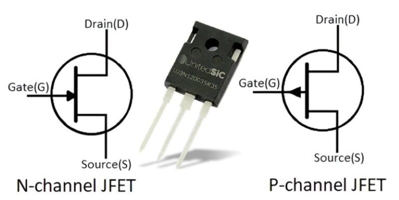
In circuit diagrams, the symbol for a JFET is distinct for N-channel and P-channel types. The arrow on the gate terminal points inwards for an N-channel JFET and outwards for a P-channel JFET, indicating the direction of current flow. The three terminals—source, drain, and gate—are labeled accordingly.
Key Features of JFET
- High Input Impedance: JFETs have extremely high input impedance, making them ideal for amplifying weak signals without drawing significant current from the input source.
- Voltage-Controlled: JFETs are controlled by the voltage applied to the gate, rather than the current, which leads to lower power consumption.
- Low Noise: Due to their construction, JFETs are known for generating very little electrical noise, which is beneficial in sensitive analog applications.
- Simplicity: JFETs have a simpler structure compared to MOSFETs, making them more robust and cost-effective in certain applications.
JFET Construction
Structure of JFET (N-channel and P-channel types)

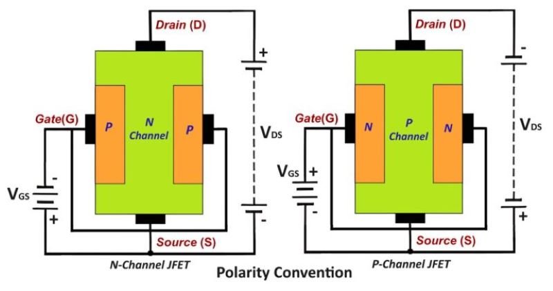
JFETs are available in two types: N-channel and P-channel. In N-channel JFETs, the majority charge carriers are electrons, while in P-channel JFETs, the majority charge carriers are holes. The basic structure consists of a semiconductor channel (either N-type or P-type) with two ohmic contacts known as the source and drain. A p-n junction is formed at the gate, which controls the flow of current through the channel.
Explanation of Depletion Region
The depletion region in a JFET is the area near the p-n junction where charge carriers are depleted due to the reverse-bias voltage applied at the gate. As the gate voltage increases, the depletion region expands, reducing the size of the channel through which current can flow between the source and drain. This effect regulates the current, allowing the JFET to act as a variable resistor.
Gate, Source, and Drain Terminals
- The source is the terminal through which carriers (electrons in N-channel or holes in P-channel) enter the channel.
- The drain is the terminal through which the carriers leave the channel.
- The gate is the control terminal, where the voltage applied determines the width of the depletion region, effectively controlling the current flow between the source and drain.
Working Principle of JFET
Operation of JFET (N-channel and P-channel)
In an N-channel JFET, a positive voltage is applied to the drain, while the gate is kept at a negative voltage relative to the source. As the gate voltage becomes more negative, it widens the depletion region, restricting the current flow between the source and drain. For a P-channel JFET, the polarity is reversed—the gate is kept positive relative to the source, and the flow of holes (rather than electrons) is controlled in the channel.
How JFET Operates in Depletion Mode
JFETs naturally operate in depletion mode, meaning that without any external gate voltage, a conductive path exists between the source and drain. Applying a reverse-bias voltage to the gate increases the depletion region, reducing the channel’s conductivity. The device continues to conduct until the pinch-off voltage is reached.
Explanation of Pinch-off Voltage and Saturation Region
The pinch-off voltage is the point at which the depletion region grows large enough to completely block current flow through the channel. Beyond this voltage, the JFET enters the saturation region, where the drain current (ID) becomes nearly constant and independent of the drain voltage. This is the region where JFETs typically operate as amplifiers.
Characteristics of Output and Transfer Curves
- Output characteristics depict the relationship between the drain current (ID) and drain-source voltage (VDS) for different gate-source voltages (VGS).
- Transfer characteristics show how the drain current (ID) varies with the gate-source voltage (VGS) at a constant drain-source voltage, typically demonstrating that the drain current decreases as the gate-source voltage becomes more negative (in N-channel JFETs).
JFET Characteristics
Drain Characteristics
The drain characteristics of a JFET describe the relationship between the drain current (ID) and the drain-source voltage (VDS) at various gate-source voltages (VGS). The characteristic curve can be divided into three regions:
- Ohmic Region: At low VDS, the JFET operates like a resistor, where ID increases linearly with VDS.
- Active (Saturation) Region: As VDS increases, the JFET reaches the pinch-off voltage, and ID becomes nearly constant, independent of VDS. This region is used for amplification.
- Cutoff Region: When the gate voltage becomes more negative (in N-channel JFETs), the depletion region widens, cutting off the current entirely.
Transfer Characteristics (ID vs VGS)
The transfer characteristics of a JFET show how the drain current (ID) changes with varying gate-source voltage (VGS). The relationship is nonlinear, with ID decreasing as VGS becomes more negative. For an N-channel JFET, the drain current is maximum when VGS = 0 and gradually decreases as VGS becomes more negative, eventually reaching zero when the channel is fully pinched off. This curve helps in understanding how JFETs control current flow using gate voltage.
Key Parameters (e.g., Transconductance, Drain Current, etc.)
- Transconductance (gm): It represents the rate of change of the drain current with respect to changes in gate voltage, given by the formula gm = ∆ID / ∆VGS. A higher transconductance means the device is more responsive to changes in gate voltage.
- Drain Current (ID): The current flowing from the drain to the source, controlled by VGS.
- Pinch-off Voltage (VGS(off)): The gate-source voltage at which the drain current reduces to zero.
- Gate-Source Cutoff Voltage (VGS(off)): The voltage beyond which the JFET enters the cutoff region, and no drain current flows.
JFET Biasing Techniques
Self-Biasing
In self-biasing, a resistor is placed between the source and ground, allowing the source voltage (VS) to rise, creating a reverse bias at the gate with respect to the source. This configuration stabilizes the operation of the JFET by making it less sensitive to temperature variations and component tolerances. Self-biasing is commonly used because it’s simple and provides stable operation.
Voltage-Divider Biasing
Voltage-divider biasing uses two resistors in series to form a potential divider between the supply voltage and ground, providing a fixed bias voltage to the gate. This technique provides more precise control over the gate voltage, allowing for fine-tuning of the JFET’s operating point. It’s widely used in amplifier circuits to ensure the JFET operates in the active region.
Gate Biasing
In gate biasing, a separate biasing voltage is applied directly to the gate, usually through a high-value resistor to limit current. This method is simple but can be less stable than self-biasing or voltage-divider biasing due to its sensitivity to temperature and component variations. Gate biasing is used when a fixed gate voltage is required.
JFET vs. MOSFET
Differences Between JFET and MOSFET in Construction, Operation, and Applications
- Construction: A JFET has a p-n junction between the gate and the channel, while a MOSFET has an insulated gate with an oxide layer separating the gate from the channel.
- Operation: JFETs are always depletion mode devices, meaning the channel is conductive by default and requires a reverse-bias voltage to reduce current flow. MOSFETs, on the other hand, can operate in both depletion and enhancement modes, with the enhancement mode requiring a gate voltage to create a conductive channel.
- Applications: JFETs are used in low-noise, analog circuits like preamplifiers and signal processors due to their high input impedance and low noise characteristics. MOSFETs, being more versatile and capable of handling higher power, are used in power electronics, digital circuits, and high-speed switching applications.
Applications of JFET
Amplifiers (Low-Noise Amplifiers, Audio Amplifiers)
JFETs are widely used in low-noise amplifiers due to their high input impedance and low noise characteristics. In audio amplifiers, JFETs amplify weak audio signals while maintaining signal fidelity, making them ideal for sensitive applications like microphone preamps and instrument amplifiers.
Switching Circuits
In switching applications, JFETs function as efficient electronic switches. Their fast response and low power consumption make them suitable for switching analog signals, especially in low-power, high-speed circuits.
Analog Signal Processing
JFETs are used in various analog signal processing circuits due to their ability to handle small signals with minimal distortion. They are often found in filters, voltage-controlled resistors, and modulators.
Use in Oscillators and Mixers
JFETs are also used in oscillators and mixer circuits due to their stability and ability to function at high frequencies. Their low noise performance ensures that signals remain clean, which is vital in communication and RF circuits.
Advantages and Limitations of JFET
Benefits (High Input Impedance, Low Noise, etc.)
- High Input Impedance: JFETs have very high input impedance, making them ideal for interfacing with high-impedance signal sources without loading them.
- Low Noise: Due to their construction, JFETs generate very little electrical noise, which is critical in precision analog applications like audio and instrumentation amplifiers.
- Simplicity: JFETs have a simple structure, making them robust and reliable in various analog applications.
Limitations (Limited Gain, Sensitivity to Gate Voltage)
- Limited Gain: JFETs generally offer lower gain compared to MOSFETs or BJTs, limiting their use in high-gain amplification circuits.
- Sensitivity to Gate Voltage: JFETs are sensitive to gate voltage, and small variations can cause significant changes in output current, requiring careful biasing to ensure stable operation.
- Low Power Handling: JFETs are typically used in low-power applications and are not suitable for high-power circuits like power supplies.
Conclusion
In summary, the JFET is a versatile and efficient semiconductor device with applications ranging from low-noise amplifiers to analog signal processing and switching. Its high input impedance and low noise characteristics make it particularly suited for sensitive analog applications, while its simple structure ensures robust and reliable performance. However, JFETs are limited in gain and power handling, and careful biasing is required to maintain stable operation. Despite these limitations, JFETs remain a valuable component in various analog and low-power electronics applications.


