Overcoming Common Annular Ring Issues in PCB Design
Annular rings play an imp role in the design and functionality of printed circuit boards (PCBs), ensuring the proper electrical connection of two pads. The placement and size of annular rings significantly affect signal integrity and current flow between PCB layers. Incorrect calculations or improper placement can lead to transient behavior and flicker noise in electronic components. This article explores the critical aspects of annular rings, including their structure, sizing parameters, benefits, types and common problems, providing comprehensive insights for PCB designers to enhance their designs.
What is an Annular Ring?
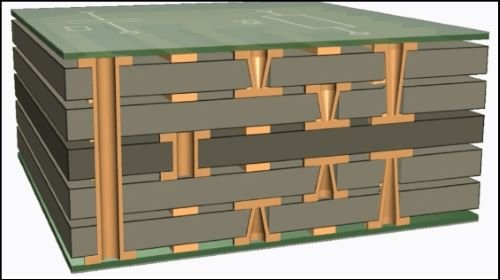
An annular ring in a PCB refers to the copper ring surrounding a hole drilled into the PCB. This hole, known as a via, connects the copper pads of different PCB layers, ensuring a reliable electrical connection. The annular ring is essentially a cylindrical copper attachment inserted through the via, forming a crucial part of the inter-layer connectivity in multilayer stack PCBs. The size and electrical properties of annular rings are determined by the PCB manufacturer’s capabilities and the specific design requirements.
Structure of an Annular Ring
Understanding the structure of an annular ring involves breaking it down into its main components and their interactions within the PCB:
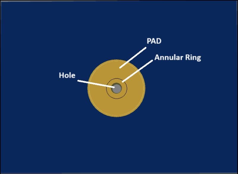
- Pad: The pad is the copper area on the PCB where the annular ring is formed. It serves as the landing area for the component lead or via.
- Hole (Via or Through-Hole): The hole is drilled through the pad and the PCB, either as a via for inter-layer connections or a through-hole for through-hole components. The hole is typically plated with copper to create a conductive path.
- Annular Ring: The annular ring is the ring-shaped area of copper surrounding the drilled hole, forming part of the pad and ensuring a good electrical connection.
Importance of Annular Ring Size
The size of the annular ring is critical for ensuring reliable electrical connections and mechanical stability. Proper annular ring width is essential for creating robust solder joints, preventing breakout during drilling, and reducing the risk of pad lifting. Key reasons why annular ring size is important include:
- Solder Joint Reliability: Adequate annular ring width ensures strong solder joints, which are crucial for reliable electrical connections.
- Manufacturing Tolerances: Properly sized annular rings accommodate manufacturing tolerances, ensuring uniform plating coverage and avoiding issues like voids or thin copper layers.
- Mechanical Strength: Sufficient annular ring width provides mechanical stability, especially in through-hole vias, preventing issues like pad lifting and breakouts.
- Compliance with Industry Standards: Adhering to standards such as IPC guidelines helps maintain high-quality PCB fabrication and enhances overall reliability.
Sizing Parameters of Annular Rings
The key sizing parameters for annular rings include:
- Outer Diameter (OD): The overall diameter of the pad, including the annular ring and the hole.
- Drilled Hole Diameter (D): The diameter of the hole drilled through the PCB, which is later plated with copper to form a conductive path.
- Annular Ring Width (W): The radial distance between the edge of the drilled hole and the outer edge of the pad.
The formula to calculate the annular ring width is:
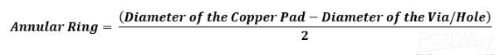
Annular Ring Width (W)= (Outer Diameter (OD)−Drilled Hole Diameter (D))/2
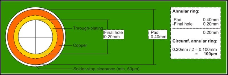
This formula helps ensure that the annular ring is appropriately sized to accommodate manufacturing tolerances and design constraints.
Design Considerations for Annular Rings
- Width: The width of the annular ring must be sufficient to ensure a good connection while fitting within the PCB design constraints. Industry standards, such as IPC-2221, specify minimum annular ring widths to help guide designers.
- Tolerances: During PCB manufacturing, tolerances for hole positioning and drilling must be considered. The annular ring should be designed with these tolerances in mind to ensure that even with minor positional errors, there is still enough copper around the hole to maintain a connection.
- Teardrop Annular Ring: A teardrop annular ring is a specialized design feature where the trace widens as it approaches a drilled hole or via, resembling a teardrop shape. This design adds strength and rigidity, reduces the risk of cracking, and provides protection against thermal stress. Teardrop annular rings are commonly used in high-reliability applications such as aerospace, automotive, and medical electronics.
Types of Annular Rings Used in PCB Design
Different types of annular rings are used to accommodate various manufacturing processes, design requirements, and functional needs:
Internal Annular Rings
Found on the inner layers of a multi-layer PCB, internal annular rings are critical for connecting different layers through vias. They must be precisely aligned and manufactured to ensure reliable inter-layer connections.
External Annular Rings
Located on the outer layers of the PCB, external annular rings are typically visible and used for mounting components and connecting component leads to PCB traces. These rings must withstand soldering processes and provide robust mechanical and electrical connections.
Microvia Annular Rings
Used in high-density interconnect (HDI) PCBs, microvias are smaller than traditional vias and typically laser-drilled. The annular rings around microvias need to be very precise to maintain connectivity in densely packed PCB layouts.
Tenting Annular Rings
In tenting, the via hole is covered with a solder mask, leaving the annular ring exposed. This method protects the via from environmental factors and prevents accidental short circuits, often used in vias that do not need to be soldered but still require electrical connections.
Common Problems with PCB Annular Rings
PCB designers may face several issues with annular rings that can impact the overall reliability and functionality of the PCB. Understanding these problems is crucial for designing and manufacturing robust PCBs:
Tangency
Tangency occurs when the drilled hole is off-center and touches the edge of the pad, disrupting connectivity and potentially causing dangerous conditions. Proper design and manufacturing tolerances can prevent tangency.
Breakout
A breakout happens when the hole pushes outside the edge of the annular ring and the copper pad, often due to poor alignment through PCB layers. Ensuring the annular ring is wide enough to accommodate the hole can prevent breakouts.
Rupture
Rupture occurs when the annular ring breaks or cracks due to mechanical stress, environmental stress, or poor quality materials. Using high-quality materials and adhering to manufacturing best practices can mitigate rupture risks.
Pad Lifting
Pad lifting happens when the pad, along with the annular ring, detaches from the PCB substrate due to mechanical stress, thermal cycling, or poor adhesive properties. Enhanced adhesion materials and careful thermal management during manufacturing can reduce pad lifting.
Final Thoughts
In summary, Annular rings are a key feature in PCB design, ensuring reliable electrical and mechanical connections between components and the PCB. Proper design and sizing of annular rings are crucial for PCB functionality, manufacturability, and long-term reliability. By understanding the structure, sizing parameters, benefits, types, and common problems of annular rings, PCB designers can improve their designs and achieve high-quality PCBs that meet industry standards and performance requirements.