IC Package Overview: Features, Benefits and Trends
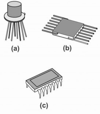
Integrated Circuit (IC) packaging plays a crucial role in protecting and interconnecting delicate integrated circuits with the external environment. These packages serve as a bridge between the silicon chip and the system it operates within, providing mechanical support, thermal management, and electrical connections. Different types of IC packages have been developed to cater to various design and application requirements. This article focuses on three widely used IC package types: Top or To Hat Package, Flat Package, and Dual-in-Line Plastic Package.
Top or To Hat Package

Description of the Top or To Hat Package Design: The Top or To Hat package is a distinctive IC packaging style characterized by its “hat-like” shape. It features a metallic lid that resembles a top hat, which encloses the semiconductor die for added protection. This design offers excellent sealing capabilities to shield the internal components from environmental factors such as moisture and contaminants.
Common Materials Used in Construction:
- Lid: Typically made of metal (e.g., aluminum or alloy steel) for durability and heat dissipation.
- Base: Ceramic or metallic materials to ensure thermal stability and structural integrity.
- Sealant: High-performance adhesives or glass to secure the lid and base.
Unique Physical and Functional Attributes:
- Hermetic sealing for enhanced protection.
- Superior heat dissipation due to the metallic lid.
- Robust design suitable for high-reliability applications.
Applications
The Top or To Hat package is commonly used in:
- Aerospace and Defense: High-reliability applications that demand resistance to extreme environments.
- Power Electronics: High-power devices requiring efficient thermal management.
- Sensors: Enclosing delicate sensor components to prevent contamination.
Advantages and Limitations
Advantages:
- Provides exceptional protection against environmental factors.
- Offers excellent thermal performance.
- Highly durable and suitable for critical applications.
Limitations:
- Higher manufacturing cost compared to other package types.
- Bulkier design may not be suitable for compact devices.
- Complexity in assembly due to the use of multiple materials and sealing processes.
Flat Package
Explanation of Flat Packages and Their Physical Structure: Flat packages are low-profile IC packages designed for applications where space is a premium. These packages feature a planar design, with the semiconductor die encapsulated in a flat rectangular or square body. The leads extend outward or downward for connection to printed circuit boards (PCBs).
Key Materials and Design Considerations:
- Encapsulation: Molded plastic or ceramic materials to protect the die.
- Leads: Typically made of plated copper or alloy for reliable electrical connections.
- Die Attach: Conductive adhesive or solder for securing the die within the package.
Applications
Flat packages are widely utilized in:
- Consumer Electronics: Compact devices like smartphones and tablets.
- Automotive: Applications requiring robust yet space-efficient packaging.
- Medical Devices: Miniaturized medical equipment and implants.
Advantages and Limitations
Advantages:
- Compact and lightweight design.
- Cost-effective for high-volume production.
- Good thermal and electrical performance for most applications.
Limitations:
- Limited heat dissipation compared to metal-based packages.
- Susceptible to mechanical stress due to the thin structure.
- Challenges in handling and assembly for very small package sizes.
Dual-In-Line Plastic Package
Description of the Dual-In-Line (DIP) Plastic Package Design: The Dual-In-Line Plastic Package is a widely recognized IC package type, featuring a rectangular body with two parallel rows of pins extending from the sides. These pins are designed to fit through holes in printed circuit boards (PCBs), providing secure mechanical and electrical connections.
Overview of Pin Layout and Standard Sizes:
- The number of pins typically ranges from 8 to 64, depending on the application.
- Standard pin spacing is 2.54 mm (0.1 inch), making it compatible with breadboards and standard PCB layouts.
- The body is made of plastic, encapsulating the die and protecting it from physical and environmental damage.
Applications
DIP packages are commonly used in:
- Microcontrollers and Microprocessors: Ideal for prototyping and small-scale production.
- Memory Chips: Early generations of RAM and ROM.
- Analog and Digital Circuits: Operational amplifiers, logic gates, and timers.
Advantages and Limitations
Advantages:
- Easy to handle and assemble, especially for prototyping.
- Compatible with through-hole PCB designs, simplifying soldering.
- Durable and cost-effective for a wide range of applications.
Limitations:
- Bulkier compared to modern surface-mount packages, leading to larger PCB designs.
- Limited thermal performance due to plastic encapsulation.
- Not suitable for high-density or high-speed applications.
Comparison of IC Package Types
Side-by-Side Comparison Table
| Feature | Top or To Hat Package | Flat Package | Dual-In-Line Plastic Package |
|---|---|---|---|
| Size | Bulky | Compact | Moderate |
| Material | Metal/Ceramic | Plastic/Ceramic | Plastic |
| Thermal Performance | Excellent | Moderate | Limited |
| Cost | High | Moderate | Low |
| Applications | High-reliability (Aerospace, Sensors) | Compact electronics (Consumer, Medical) | Prototyping, Analog/Digital Circuits |
Discussion of Key Differences
- Size and Compactness: Flat packages are the most compact, making them ideal for portable electronics. DIP packages are bulkier but easier to handle.
- Thermal Management: Top or To Hat packages excel in heat dissipation, while DIP and Flat packages are suitable for low-to-moderate thermal requirements.
- Cost: DIP packages are the most economical, followed by Flat packages. Top or To Hat packages are costlier due to their robust construction.
- Applications: The choice of package depends on the balance between reliability, size constraints, and cost.
Emerging Trends and Future of IC Packaging
Advances in IC Packaging Technology
- System-in-Package (SiP): Integrates multiple components into a single package to save space and enhance functionality.
- 3D Packaging: Stacks multiple dies vertically for improved performance and miniaturization.
- Fan-Out Wafer-Level Packaging (FOWLP): Offers high-density interconnections with a thin profile.
Integration of Modern Techniques into Traditional Packages
- Incorporating advanced materials like thermally conductive plastics.
- Enhanced leadframe designs for better electrical performance.
- Automation and precision in assembly to reduce costs and improve consistency.
Final Words
IC packaging continues to evolve, driven by the demands for miniaturization, higher performance, and cost efficiency. Top or To Hat packages offer unparalleled reliability for critical applications, while Flat packages serve compact devices with space constraints. Dual-In-Line Plastic packages remain a go-to choice for prototyping and cost-sensitive projects. By understanding the strengths and limitations of each package type, designers can make informed choices that align with their application’s needs and constraints. The future of IC packaging promises further innovation, ensuring that new designs meet the growing challenges of modern electronics.


